Quy trình DTFS là gì?
Semiconductors are the fundamental building blocks of the electronics industry. These partly conductive goods include transistors, processors, and other electronic control pieces that are used in everything from mobile phones to automobiles and robots. Today, most semiconductor chips are made from silicon coated with another compound.
This outer layer shields the semiconductor from the elements while keeping it connected to the outside world. Plating materials can range from tin to gold, with different sets of characteristics that bring along varied results. Surface finish standards in the semiconductor business are among the most demanding of any industry that utilizes our services.
The industry has set stringent requirements for an acceptable finish quality due to the corrosive nature of the liquids and gases used in manufacturing. Electronic packaging is being manufactured in greater numbers than ever before. Even though the manufacturing of these packages is continually increasing, issues with cutting quality and speed remain unsolved. The various mechanical, thermal, optical, and electrical characteristics of the materials involved are the underlying factors.
A copper lead frame or a thin glass fiber-enhanced polymer circuit board with solder balls is a common material used for the substrate. It is to be soldered to the final circuit board and the mold compound to protect the chip. The contacts with the substrate are the two basic materials used in electronic packaging. The mold compound is typically a brittle, black polymer with various filler components.
In the years to come, the semiconductor industry will face the difficulties and possibilities of growing demand for semiconductors. The semiconductor supply chain will be under pressure from continuous demands from the smartphone industry and other high-tech businesses, and also as artificial intelligence and the Internet of Things become more prevalent. This problem will be exacerbated by current international trade tensions, which might inflate the material cost and stymie global industry collaboration. New solutions are necessary to fulfil these demands. It remains a challenge to build semiconductor devices utilising more environmentally-friendly procedures and to recycle materials at the devices’ end-of-life.
The DTFS process consists of three stages,
- Deflash
- Trim and Form
- Singulation
Edge finishing, deburring, and Deflashing are time-consuming and expensive steps in the production process. The prices might vary greatly depending on the produced products and the level of accuracy required to complete those items. Flash or Burr removal accounts for 32% of the manufacturing cost for some items.” According to the DESA 2012 laureate Laroux K. Gillespie, Mechanical Engineering, the type of material used, the size of the components, and the type of parts (precision, close-tolerance, medical, aviation, and so on) are to be taken into consideration when determining the finishing costs. Burrs and Flash removal may account for just 5-10% of the fabrication cost for some manufacturers. However, in terms of total fabrication costs, that might still be a significant amount.
Deflash Process:
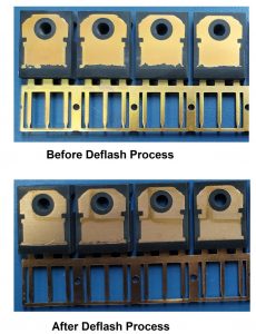
Deflashing is an important step during its’ production stage in the semiconductor industry. An acid solution is used to remove excessive encapsulating material from unmolded areas of a molded substrate incorporating semiconductor packages. It simply refers to the removal of excess mold leak or bleed and resin bleed caused by the molding process during the assembly of plastic devices. Mold bleed is a result of leaks and is black in colour, whereas resin bleed is caused by the separation of the epoxy resin from the fillers and is translucent/light yellowish-brown. By using a chemical-free deflash process, the lead deflash method allows for the total eradication of lead flash created during package production, as well as serving as a pollution deterrent.
During the molding process, small amounts of resin leak out from between the two halves of the mold under the pressure, resulting in a flash. A self-supporting opacity film projected around the body of the package at the point where the halves were connected. Molding flash appears when the optimal parameters of the equipment are not calibrated. Mold separating surface design can reduce or eliminate flash. Molding flash can occur from old or worn mold cavities that no longer fit tightly together. At times, the part’s intricacy necessitates the use of many matching components with such precise geometries that it is nearly impossible to get a good fit on every impression. Most of the time, the type of material being molded, and its accompanying viscosity in liquid form, is the primary reason for the formation of undesirable mold flash. Formation of the flash during the manufacturing process at be attributed to various factors such as,
- Difference in the flatness of the molded surface
- Change in the dimensions of lead-frames
- Distortion due to varying temperature
- Change in the parameters of the molding process
- Variation on the clamping force applied by the press
- Small tolerance in thickness of the lead frames.

There are four types of Deflashing techniques used in the semiconductor manufacturing process,
- Dry Blasting
- High-Pressure water jet process
- Chemical Deflash process
- Wet Blasting
Dry Blasting:
Dry Ice Blasting is a unique sandblasting technique that is noted for its excellent efficiency. It is a non-abrasive cleaning method that removes surface impurities without the use of chemicals, abrasive materials, high temperatures, or steam. The solid pellets dissolve instantly after impact on the surface, leaving no solid behind. This approach is suitable for surface cleaning, paint removal, and the eliminating of pollutants from a surface. Dry Ice Blasting, unlike other blast cleaning methods, does not collect pollutants in the waste stream and is a considerable reduction in secondary waste.
Sand Blasting is an example of an abrasive treatment technique. It involves the use of abrasive particles in a stream of compressed air or liquid to clean or shape the workpiece’s surface. Sand Blasting can provide a surface with specified roughness attributes for future adhesive bonding procedures by changing the applied stream pressure and grit diameter to the specific substrate material. Sand Blasting is commonly done using Silica sand, although alternative media such as broken glass, metal particles, dry ice particles, garnet, coking slag, and glass or ceramic beads can also be used.
Thermal shock and pneumatic effect are two contributing variables to the method’s success. The collision of dry ice particles compresses the surface contamination, which then experiences thermal shock due to the large temperature difference (dry ice temperature is 79°C), causing it to separate from the surface. The jet stream’s high velocity effectively scrubs loose material away. Dry Ice particles convert to gas and sublimate completely into the environment shortly after being released.
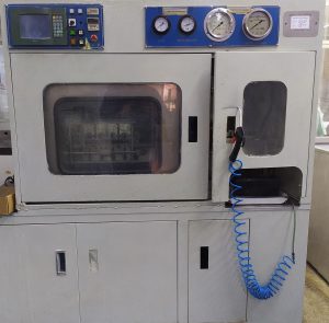
Dry Blasting equipment such as Hunzikar Thermoset Deflashing Equipment.
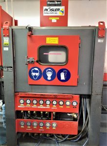
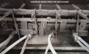
The Dry Ice Blasting process has several benefits:
- Dry Ice particles transform into CO2 gas and sublimate into the environment when coming into contact with surface contaminants, resulting in no waste management issues.
- Blasting with dry ice media is ecologically friendly as it does not involve the use of any extra chemicals. The surface pollution that is removed is the only by-product of the operation.
- Due to its non-abrasive nature and the absence of compounds preventing corrosion resistance in the mix, the procedure is completely safe for the substrate surface.
- Dry Ice Blasting has little effect on the operation of machine parts. Most of the elements may be cleaned without disassembling.
- The procedure is time-efficient: surface preparation is easy, and the surface after Dry Ice blasting is always free of contaminants.
- Sand Blasting equipment is rather simple to operate. No additional training or knowledge is required.
- Sand Blasting machines’ excellent functionality can be attributed to their design (a system of unique nozzles and extensions), which ensures consistent quality in a variety of, even adverse, working situations.
High Pressure Water jet Process:
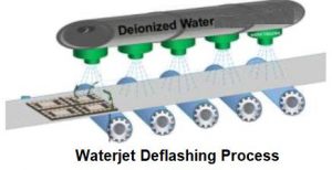
Water jet cleaning, also known as wet blast cleaning, is a common method for removing debris, coatings, and burrs from a surface. Progressive Surface specializes in ultra high-pressure water jet stripping and has experience with all kinds of water jet procedures. The water jet cleaning procedure has several advantages over rival traditional burr or flash removal processes. Burr or flash removed using ultra high-pressure water was traditionally removed with chemicals or other traditional mechanical methods like abrasive blasting or machining. Chemical cleanup is costly, time-consuming, and harmful to the environment. Comparatively, chemical processing is more cost-effective and efficient. However, abrasive blasting or milling cannot distinguish between the coating and the substrate. This results in excessive material loss and reducing the lifespan of these components. Water jet stripping is ideal for coating removal for essential applications like removing thermal sprayed coating off industrial gas turbine components as it is rapid, ecologically benign, and can remove the coating with minimum to no substrate loss.
There are a variety of washing procedures that may be used with a water jet and the best ones should be chosen based on the work arrangement and the state of the burr. Nozzle types, moving nozzle techniques, jetting circumstances, cleaning atmospheres, and other variables are among the parameters. Ultra high-pressure water jet stripping uses water that is pressured between 30,000 and 60,000 psi to remove coatings and debris from substrates.
These coatings are removed by using one of two mechanisms: erosion or delamination. The bulk of hard coatings, such as metal and carbide thermal spray coatings, are destroyed. The water stream is broken up into little droplets by a specific nozzle, which strikes the coated surface. Small bits of the covering dissolve away from the surface, leaving the substrate unharmed. The following subsystems are found in most water jet systems:
- Pressurize the water with a pump.
- Nozzle for delivering the proper water stream to the work piece
- Enclosure to keep the process contained
- Manipulators for nozzles and parts
- Waste-handling machinery
- Control devices for the process
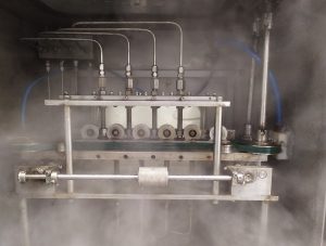
High pressure Waterjet equipment such as Jastech waterjet machine.
Chemical Deflash:
For the chemical removal of resin bleed from synthetic epoxy semiconductor devices, molded parts are first deflashed, simultaneously removing encapsulating material from between adjacent leads and removing those sections of the lead frame that hold the leads fixed during the molding operation. The lead frame is then cleaned and chemically treated by soaking it in a solvent for the encapsulating resin, long enough to eliminate the resin bleed but not long enough to harm the resin encapsulation. The device is cleaned once the resin bleed has been removed, and the lead frame is then plated or solder-dipped.
Chemical deflashing is the soaking of components in materials like methyl pyrrolidine, with additives to prevent soils from re-depositing on the devices and surface-active agents to expedite penetration and facilitate quick removal of the residue. Soaking can be done at a high temperature and with the aid of ultrasonic. The dissolved residue is removed by blasting with compressed air, high-pressure water, or abrasives after a water rinse. While chemical deflashing is successful, there is some risk that the compounds employed in it may leak into the packaging and cause the device to degrade. Some of the chemicals utilised are also dangerous, and may pose waste disposal issues.
Wet Blasting:
Wet blasting is different from dry blasting. It uses a third ingredient – water – to improve the amount of surface finish. The use of water results in a more uniform and smoother finish. To deflash the components, wet blast systems employ slurry of water and abrasive materials. Hard materials, such as aluminum oxide or glass beads, can be utilised since the water cushions the impact of the media. This technique reduces dust and static damage, resulting in cleaner components. Impregnation, surface degradation, and excessive media breakdown are avoided as there is always a cushion of water between the media.
There are five characteristics for Wet Blasting,
- Particle size, shape, and material quality are all available in a wide range.
- Excellent fluidic controllability performance.
- Particle residual errors are minimal.
- Thinner materials can be used.
- Chemical mixtures can be used for secondary processing.
Following are some different parameters we try to control:
- Air pressure control
- Volume of air control
- Slurry pressure
- Water temperature
- Water pH
- Water conductivity
- Filtration
- Rinsing
- Drying
- Gun angle
- Gun range
- Media concentration
- Process speed
Trim and Form:
Trim and form is the process of separating the leadframe’s leads from the leadframe strip. The Dambar that electrically isolates the leads is first removed during the operation is known as trim process. The leads are then inserted into tooling, chopped, and mechanically molded into the desired shape is known as form process. For surface-mounted plastic packaging, J-bend and gull-wing forms are utilised. Straight lead, J-lead, and gull-wing lead are different types of leaded IC packages. A typical example of a straight lead package is a plastic dual in-line package, which is mostly used for through-hole PCB fabrication. Plastic leaded chip carrier commonly uses J-lead shaped profiles. Quad flat pack and thin tiny outline packaging both have gull-wing shaped leads. Individual units are separated from the leadframe strip and put in trays or tubes after being tested for lead co-planarity. To produce the coplanar leads necessary for surface mount procedures, the lead forming process is crucial. It is critical to clean tools during maintenance to ensure that the procedure is of high quality. Lead tip burrs, solder scratches, and solder cracks are the main problems for lead visual quality. The lead profile quality requirements includes:
- Co-planarity
- Lead skew and lead offset are two sub-categories of lead position.
- Lead spread
- Stand-off height
Profile projectors or optical lead scanners are frequently used to measure co-planarity. It is the perpendicular distance between the lowest resting plane and the highest lead. In most cases, based on tooling outflow requirements, the maximum co-planarity limit will not exceed 0.050 mm. If burrs from cutting are excessive, the Dambar trimming design may impact co-planarity. The width of the lead at the Dambar area may change if the dam bars are cut alternatively, and the burrs produced might be in an alternating pattern. As a result, the lead cross section varies from place to place, causing varying degrees of spring-back after forming.
The deviation of a produced lead from its theoretical position as determined in respect to the package’s centre line is known as lead skew. Profile projectors or optical lead scanning devices are commonly used to measure it. When the package is mounted to the PCB, it will change the placement of the package’s lead footprint. Depending on the packaging type, lead skew should not exceed 0.038 mm. Molding, dam bar cutting, shaping, and the lead arrangement are contributing elements to lead skew. The Dambar trimming procedure is one of the primary causes of lead skew. Dambar can be trimmed in two ways for fine pitch products: periodically or all at once. While alternating trimming results in stronger punch and die designs, it can cause serious lead skew issues during the forming process.
During the assembly process, lead trim and form procedures are frequently used to place the sensor precisely at the operational position and shape the leads to secure electrical connections by soldering on the PCB. During the trim and form procedures, significant forces are applied without the necessary protections. The applied force may act as a stress factor on the sensor’s plastic body or leads to the plastic body. Such stress may result in device failure, crucial parameter drifts, or the introduction of a reliability risk, such as,
- Stress applied to the package’s side may damage the silicon structure.
- Stress on the leads in respect to the plastic body might result in wire bond damage, package cracks, or leadframe delamination. If cracks and delamination do not cause immediate failure, they will further weaken the wire bonds, allowing moisture to penetrate and bond to corrode.
Lead Clamping:
- During the trim or form operation, the package stress relief must be achieved by firm clamping of leads from both sides.
- On both sides of the component pins, the stress relief clamp must have a minimum pressing surface width of 0.4 mm.
- It is important to make sure the clamping force is strong enough to hold the component pins in place without harming the leads. When clamping and cutting/bending pneumatic cylinders are utilised, the clamping cylinder’s force must be at least three times that of the cutting/bending cylinder.
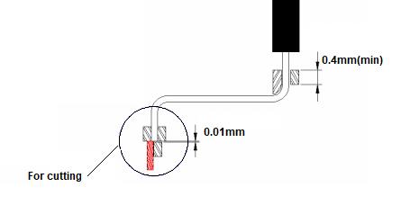
For Trimming:
- Make sure the cutting blade clearance is not too wide; otherwise, the cutting blade may flex when trimming. For soft materials like copper, a clearance of 10% of the material thickness can be used.
- Only soft cutting should be used; for example, components should not fly away from the cutter. After cutting, the best way is to release clamping.
- A basic cutter is shown with pre-acting clamping. The spring force should be calculated appropriately.
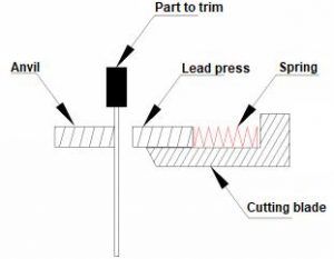
For Trimming:
- Lead formation must take place beneath the Dambar cutting section. Lead formation that falls into the zone of the tie bar should be avoided as a smooth radius is difficult to achieve in this region.
- Lead spring-back must be removed by over-bending or bottoming the leads, not by mechanical deformation.
- Clamping markings should be evaluated after processing as a process quality and tool tiredness indication. It should not reflect exposed base leadframe material or plating peeling.
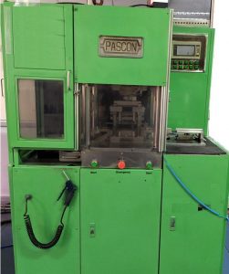
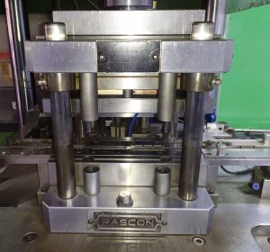
Trim and Form equipment such as Pascon TrimForm.
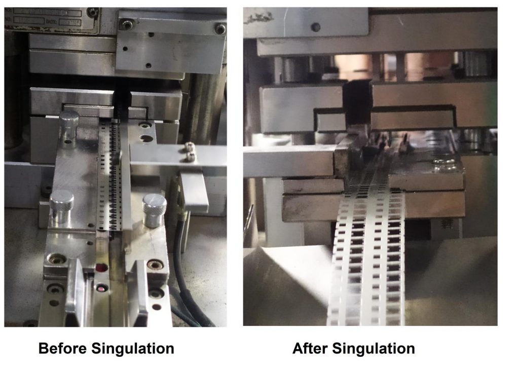
Singulation:
The Singulation method utilises an array of molded components on the upper surface of a lead frame. Between the molded components, the lead frame includes several Dambars. A tape is used to secure the lower surface of the lead frame. A semiconductor chip is enclosed in a package body and electrically linked to the upper surface of the lead frame in each of the molded products. The Singulation approach involves etching the upper surface of the lead frame while using the package bodies as a mask until each Dambar is removed.
In the case of copper and mold compound variants, cost-effective and high-quality Singulation is extremely tough. To increase productivity, this sort of package is frequently produced using a matrix-array technique. During the Singulation process, however, both the mold compound and copper materials must be cut at the same time. Cutting the entire package is a big challenge as a precise, burr-free Singulation of copper is already a challenge. Mechanical sawing and traditional laser cutting are today’s standard Chip Scale Package Singulation technologies. The intrinsic softness of copper causes burr development and quick saw blade wear due to smearing. Burr formation can make soldering the package to the board problematic at times.
