Quá trình thái hạt lựu là gì?
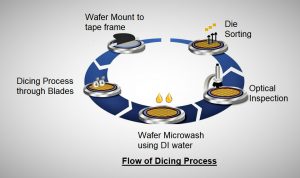
There are various steps involved in the Dicing process listed below:
- Wafer Mount to the Tape Frame
- Dicing Process Through blades
- Wafer Microwash Process
- Wafer Inspection and Die Sorting
The below image is showing the flow diagram of the Dicing process.
What is the Dicing Process?
The Dicing process is mostly used in the semiconductor packaging industry to separate Silicon wafers into individual chips. The Integrated Circuits are manufactured in a multistep process that converts raw materials into packaged devices that may be configured into electronic circuits. In other words, it is a process by which the separation of the die from the silicon wafer is referred to as the Dicing process. During the Dicing process, Wafers are mounted using PVC or Mylar tape, which has a sticky backing and holds the wafer on a metal frame. Because even the smallest dust particles might damage the complicated circuits imprinted on a wafer, the process is done in a clean area with air constantly circulating. This tape has different properties depending on its application. For smaller die sizes, UV curable tapes are used, while non-UV dicing tape is used for bigger die sizes. When a wafer is diced, the die remains on the Mylar tape until it is retrieved by the equipment, such as a die bonder. The dies are most commonly rectangular or square. Depending on the Dicing method used, they can also be other shapes.
This process involves mechanical sawing, laser cutting, scribing, and breaking. The formation of chipping and blade yielding are the two basic limitations in the dicing process. A special monitoring method is recommended for determining the maximum feed rate without exceeding these limits. To ensure precision, quality, and accuracy, all techniques are usually automated. The organization has embraced continuous improvement and development to meet customer demands. To remain competitive in the face of change, precise and robust methods are implemented to ensure that the actual units produced are of high quality and reliability. In terms of pre-assembly operations, it is necessary to optimize chippings to increase die strength during package construction, which has a direct impact on package dependability and quality. Through the analysis of key parameters and the research, synthesis, and summation of data from many sources, the analyst provides a complete picture of the market. The following areas are discussed in the analysis on the wafer dicing saws market:
- Market size for wafer dicing saws
- Market forecast for wafer dicing saws
- Market industry analysis on wafer dicing saws
Check out our article where we compare Saw Dicing, Laser Dicing, Plasma Dicing, and Scribing Dicing.
The extensive vendor research is aimed to assist clients to enhance their market position, and it includes
The market study report for wafer dicing saws also provides information on future trends and challenges that will affect market growth. This is to assist businesses in strategizing and focusing on all upcoming growth prospects.
Chipping-related problems could be reduced by providing a consistent and usable set of parameters, thus reducing their impact on total package dependability. Furthermore, the possibility of associated defects being relayed to various wafer technologies and subsequent packages might be eliminated. Wafers are classified according to which technology family they belong to. Every wafer technology classification uses a different set of indirect materials and parameters. As a result, established processes must be followed within similar wafer technology to assure a positive response based on previous experience and data-driven analysis. The worldwide dicing equipment market was worth USD 567 million in 2020, and is predicted to grow to USD 825 million by 2026, with a CAGR of 6.5 percent during the forecast period from 2021 to 2026. The increasing attempts to make electronic packaging very resourceful as a result of the huge demand for electronic components as a result of increased demand has made electronic packaging useful in a wide range of applications.
The dicing equipment market is getting pace due to the integration of microelectronics in consumer electronics. The demand for thin wafers is being driven by the necessity for technologies such as MEMS devices and power devices. Furthermore, this need supports the desire for improved manufacturing methods, which is a critical stage in the ultra-thin wafer manufacturing process. Radio Frequency Identification, MEMS devices, and power devices are considered to be the primary sources of demand for very thin wafers. This scenario is increasing demand for a better manufacturing process, specifically for processing and dicing, which are crucial stages in the creation of ultra-thin wafers. The below factors are driving the semiconductor and IC packaging markets ahead. The expertise gained in pre-assembly in improving backside and topside chip-out for silicon wafers during the qualifying run and evaluation is detailed here.
1) The increased demand for electronic items has pushed the electronic packaging sector, and customer expectations about the features of new electronic gadgets have risen.
2) The growth of IoT and connected devices, as well as smart devices, has completely dominated the electronics market. Aside from smart phones, connected wearable devices are projected to gain popularity.
- Dicing Saw equipment such as Disco DAD 321, Disco DAD 323, Disco DFD 6363, Disco DFD 6341, and Accretech AD3000T-plus and various precision tools are used to accurately cutting the wafers.
- The Wafer Mounter equipment such as Nitto M286N/M265N, Nitto MSA840P, UVFAB FM-2246, and UVFAB FM-2248.
- Sawed Wafer Cleaner equipment such as Kulicke &Soffa 971 Microwash, and Micro Automation 2006 model.
1. Wafer Mount to the Tape Frame:
Plasticized PVC film adhesive tape has been one of the most reliable products used in semiconductor device assembly and handling. It is commonly used in wafer scribing, sawing, and fracturing, wafer die row expansion and die transport and bonding. With the extensive and rising use of processing tape with a wide range of application characteristics, the user benefits from understanding the fundamentals of defining and working with tape. The success or failure of using plasticized PVC film tape for semiconductor processing is decided by whether the correct tape is utilized. Tape quality can be classified into three categories: industrial, electronic, and select. The tape grade is decided by the level of adhesion, material thickness, and flexibility in the X and Y directions, as well as the degree of uniformity.
The Wafer Tape Mounting is the process that is performed during the die preparation of the wafer. It is a part of the semiconductor fabrication process. In this process, the wafer is mounted on the tape that is attached to the metallic frame. In most cases, the Wafer Mounter area is kept at the temperature of 32°C to 38°C. The proportional–integral–derivative controller is used in this equipment to control the temperature according to manufacturing process requirements. When the wafer mounting process is completed then the temperature should be back between 32°C to 38 °C. The tape becomes more flexible at this temperature, allowing for a uniform and conformal wafer contact. The tape expands and then compresses as it cools, resulting in uniformly distributed tape tension on the wafer in the film frame. If the tape’s elasticity is uniform, this effect will occur.
The amount of tension in both the X and Y directions must be equal. As a result, the mounting system should include a method for equally supporting the tape as it is mounted around the edge of the film frame. When the tension is released on the second saw cut, the incorrect amount of tension in either direction causes load shifting, resulting in crooked die rows. The tape should not be sawed right after it has been mounted. To enable time for the process to settle and produce uniform adhesion, let about 30 minutes of dwell time between the mounting and dicing processes. Every film frame should have the same time interval. The process is started by placing the wafer face down in the tape applicator and positioning it using the concentric circular grooves. Then, place the film frame around the wafer with predefined pins on the Mounter surface. Pull the roller over the wafer by the handle and the wafer will mount on the metallic frame as shown below.
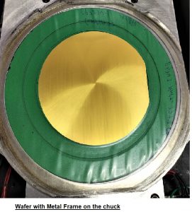
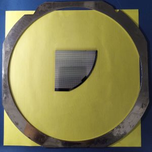
After the tape mounting process, cut the excessive tape with the cutter, and then unloading of the mounted wafer process occur. The below image is showing the wafer is mounted on the metal frame.
During the wafer mounting process, there are some necessary steps to be followed.
- It is important to handle the wafer with care to prevent wafer cracking or any breakage.
- Protect from the bubble traps on the adhesive side of the tape.
- Protect from scratches on the active side of the wafer.
- Protect from tape wrinkle.
2. Dicing Process through blades:
Various processes can be performed using blade dicing saws functions as below,
- The most basic processing method is full cut, which completely cuts the die up to the securing material, such as dicing tape. Wafer dicing is the most well-known semiconductor manufacturing process. All dicing saws are capable of completing this task.
- Half-cut is a grooving technique that involves cutting the workpiece up to the middle and then grooving it. Half cutting is utilized in the DBG process in semiconductor manufacturing, which is a process in which grooves are first created by half cutting, then thinning and die separation, which is done at the same time by grinding.
- Dual-cut is a method that uses a dual dicing saw with two spindle axes to do the full or partial cutting for two lines at the same time. With this method, a high throughput can be achieved.
- Step cut is a processing method that uses a dual dicing saw with two spindle axes to do full and half cutting in two phases.
- V-shaped cut is a processing technique that involves cutting the wafer in two steps using a blade with a V-shaped edge on the half-cut side during step cut. As a result, high die strength and high-quality processing are possible.
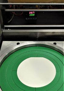
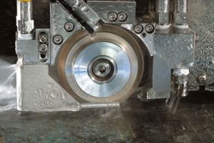
Wafers are mounted on Mylar tape, which has an adhesive backing and is used to hold the wafer on a metal frame. The wafer frame is clamped on the vacuum chuck of the dicing saw. The wafer is placed on the chuck area and inserted into the spindle area where an abrasive diamond blade rotates at 15,000 to 30,000 RPM. As the blade rotates, the abrasive chips away at the wafer. DI Water is applied to the blade to remove cutting residue and improve cut quality. The DI water pressure should be 40 to 100 psi.
The Spindle speed should be between 15000 to 30000 RPM. Sharpening diamond particles are coated in a diamond bond matrix to allow them to freely enter the material, minimize loads, and provide good cut quality. Another reason for dressing blades is to remove material that is filling the pores between the abrasive particles on a loaded blade. The diamonds must be fully protruded and exposed to easily enter the material being cut. Poorly dressed dicing blades tend to push the material, resulting in high loads, high cutting temperature/heat, and poor cut quality. This can probably result in blade breakage.
The various parameters of high-quality cutting of the wafer are listed below:-
- The thickness of the blade depends upon the blade exposure and it should be less than Kerf width. If the exposure is more, then the sawing process requires a thicker blade.
- The exposure of the blade should be between 0.510 to 0.890 mm. It should be greater than the cut’s depth.
- The diamond’s grit size should be between 3 to 5um. For cutting very hard materials, larger diamonds are preferred. A better cut is attained with smaller diamonds.
- The cutting blade height should be between 0.0889 to 0.1397 mm.
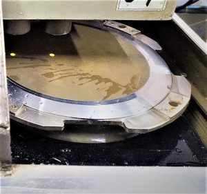
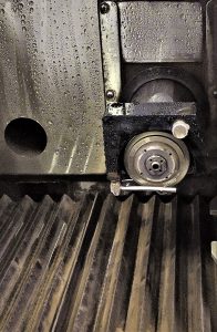
The below images show the chuck area and the spindle area of the machine.
3. Micro-wash Process:
Industry wants a technique that removes pollutants and impurities from semiconductor components without destroying the wafer, such as alkali, metals, heavy metals, and organic contaminants. The wafer’s performance and functionality may be harmed if they are not removed.
Cleaning semiconductor wafers is therefore an important stage in electronics manufacture, with a market of $7 billion by 2024. Pre-diffusion cleaning, particle removal, metallic ion removal, film removal, and a post-etch clean are some of the steps involved in cleaning semiconductor wafers utilizing wet chemistry-based cleaning technology and etch cleaning technology. Wafer cleaning is one of the most frequently performed processes throughout the wafer fabrication process. Cleaning processes are becoming increasingly challenging as technology evolves and devices shrink in size. The cleaning process should not only be performed on the wafers but also on the machinery and equipment used. Wafer contaminants include the size range of particles from 0.10 to 20 microns, organic and inorganic pollutants, and impurities. Cleaning procedures are classified as either wet or dry. Wet cleaning does require the use of solvents, acids, or water. In comparison, dry-cleaning use lasers, aerosols, or ozonated chemicals.
This process is used to clean the wafer after the dicing process. Deionization (DI) water is used to perform this process. The removal of impurities and particles that may have been deposited on the wafer surfaces or may have been left over after wafer operations must be accomplished. This must be done to reduce the possibility of defects in the final products. Unwanted particles or contaminants may block the surfaces where etching will take place, resulting in unsatisfactory outcomes.
There are two stages in which the wafer cleaning process is performed. In the first stage, DI water is applied with pressure between 100 to 150 psi to the wafer which is held with the metallic frame. In the second stage, heat is applied to the wafer to dry it. The processing time for both stages should be 3 to 5 minutes. The time setting is done by the user according to their process requirements.
The important parameters for the wafer washing process are listed below.
- The wash time of the wafer and the rotation per minute of the chuck.
- Deionization (DI) water pressure during the washing process of the wafer
- Dry time and Wet time of the wafer
- Temperature requirement during the dry process
- Air-flow rate
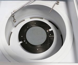
The below image shows the Micro-wash equipment Ultra-T Equipment.
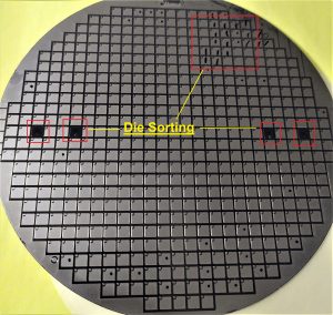
4. Wafer Inspection and Die Sorting:
The die sorting and inspection system inspect dies before assembly, allowing users to rapidly identify any errors during the dicing process of wafer-level packages. Wafer-level packaging technologies have evolved, introducing new materials into the process that can crack during dicing, such as low k materials in fan-in wafer-level packages. This solution helps chip makers reduce production risk by detecting defects rapidly during die sorting, resulting in higher outgoing quality to the next phase in the assembly process. Wafer inspection, the technology of detecting faults on a wafer, is becoming more difficult, challenging, and expensive with each node. This is owing to process shrinkage, design difficulties, and the introduction of new materials. Furthermore, using today’s optical inspection equipment, detecting sub-30nm defects is most challenging. Wafer inspection is divided into two categories: Optical systems and E-beam inspection. Both styles are usually seen as complementary, yet there are significant drawbacks. Optical examination instruments are quick, but their resolution is limited. Single beam, e-beam inspection technologies provide more resolution but are slower. Some suppliers are working on the development of a new type of multi-beam e-beam inspection system. These technologies promise to discover microscopic defects rapidly than today’s single e-beam instruments by utilizing multiple beams.
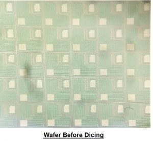
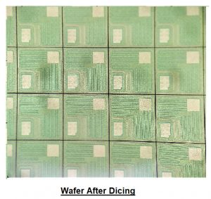
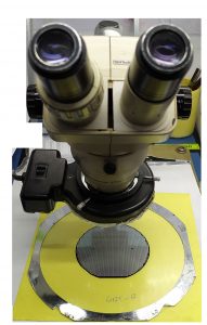
Wafers can be checked either before or after dicing. Optical inspection of the wafer is used to remove the visually damaged die. These defects might have been introduced during fabrication or as a result of physical mishandling in post-fabrication activities. The majority of visual inspections are performed by automated equipment, while manual inspection techniques are sometimes used as well. This process is used to check the die rejections on the wafer after the Dicing process. This process is performed by using a microscope. The various problems like edge chipping, cracking, and layer peeling mostly occur after the mechanical saw process. While all die on a single wafer is expected to be identical, a significant number usually fails to meet requirements.
The individual die is classified as passed or rejected, and the information is saved in an electronic wafer mapping software. The rejected die may also be marked with ink dots. Capturing images may also be used to provide rapid feedback. The rejected dies are marked with Rotring Zeichentusche drawing ink and the die bonder equipment ignores the inked die during the Die attach process using the wafer mapping technique.
You might also want to check out another article in our blog, which talks about the Die Attach Process. Is there anything we can help you with? Contact us now to find out more