Cắt bằng cưa so với Cắt bằng laze so với Cắt bằng plasma so với Cắt bằng nét chữ
In this article, we compare the differences between Saw Dicing, Laser Dicing, Plasma Dicing, and Scribing Dicing. The thin wafer dicing equipment market may be divided into four categories based on dicing technology:
A wafer is a thin slice of semiconductor material, and dicing is the process of cutting semiconductors, glass crystals, and a variety of other materials. Dicing equipment is an instrument used in this operation. Because of the increasing need for smaller wafers and tougher die, dicing technologies are continually changing, having a substantial influence on the dicing equipment sector. Grinding is another process that reduces wafer thickness to meet the demands of many sectors such as electronics, automotive, and communication devices, among others. Thin wafer handling process is done by attaching to a metallic wafer frame, which provides mechanical support during wafer dicing and backside processing. The thin wafer is separated from the carrier wafer and mounted to dicing tape on the film frame after backside processing. MEMS devices, Radio Frequency Identification, and power devices are thought to be the primary sources of demand for very thin wafers. Chemical mechanical polishing and other innovative technologies are increasingly being introduced into the processing step alongside grinding operations.
The growing adoption of wafer dicing saws in the semiconductor industry is growing the market of the wafer dicing saws market. In the forecast period of 2020 to 2027, rising demand for IoT and the number of semiconductor devices required for data centers, as well as an increase in self-driving cars, will be some of the primary drivers driving the wafer dicing saws market growth. Wafer dicing saws market expansion will be aided by rising demand from emerging economies and the development of laser wafer dicing saws. The high cost of device maintenance is a major hurdle for the thin wafer dicing equipment market. The thin wafer dicing equipment market is divided into logic and memory, micro electro-mechanical systems, power device, radio frequency identification, and image recognition sensors. The wafer dicing saws industry is highly consolidated, and vendors are competing with a variety of organic and inorganic growth strategies. The study examines the competitive landscape of the industry and provides details on many key vendors, including:
1. Wafer Scribing and Breaking:
The term Scribing is used in the semiconductor industry to describe Die Singulation. The Saw dicing process can be replaced by scribe and break die separation. Thin silicon wafers, hard materials such as sapphire, glass, and ceramics, and ultra-clean devices all benefit from the features of scribe and break die separation. The goal of this technique is to improve yield while reducing individual die handling, reducing labor costs, and processing time. To dice the wafer and release and dry the individual bits, the current procedure takes many days. The wafer is released, dried, and singulated in just one day using this innovative procedure. Due to the challenges with the current release and die singulation method, various die separation techniques have been investigated. Post-release wafer sawing, pre-release wafer sawing, laser scribe-and-break, and mechanical scribe-and-break are examples of these techniques. A successful post-release separation method must be clean, dry, quick, and consistent. The term “cleanliness” relates to reducing the number of particles produced by a process. Any particles generated could become lodged in a surface micromachine, jamming or damaging it mechanically. Because fragile surface micromachines can be easily drawn together by the capillary forces of drying liquid, the process must be dry, and speed and reliability are always concerns in mass production. There are various advantages of the Scribing process,
- No heat required
- Dry process
- Zero cutting width
- Smooth and clean-cut surface
Scribing and breaking wafer separation processes are performed by inducing stress in the wafer and then fracturing it along the stress line. To break the wafer, a scribe line must be formed in the wafer surface along the streets. As a result of the stress concentration factor created by this line, the wafer breaks along it when force is applied. The stress concentration factor is created by a combination of the wafer’s reduced cross-sectional area and the sharpness of the scribe line’s bottom. The sharpness of the scribe’s bottom has a significantly greater impact on the stress concentration factor than the scribe’s depth. Scribe methods that create the stress concentration factor mostly do so by reducing the wafer’s cross-sectional area. By reducing the cross-section of the wafer when scribing with a saw, the saw creates a stress concentration factor. The thickness of the wafer is often reduced by 50 to 70 percent. There are two ways that laser scribes reduce cross-sections. The first is comparable to a saw in that it makes a continuous cut along the street at a specified depth. The second method, which is more common for ceramic wafers, involves pulsing a series of holes through the wafer spaced an equal distance apart. The scribing and breaking process is not the best solution in every situation. The scribe-and-break This method of splitting silicon wafers into die was widely used in the semiconductor industry until it was replaced by dicing in the late 1970s and early 1980s. Dicing has mostly replaced scribe-and-break because it is less dependent on die size, wafer thickness, the ratio between die size and thickness, crystal plane orientation, and the materials and structures in the streets.
In this technique, the wafer is partially cut through by one process tool. The scribe line is created on the wafer surface as a result of this process. The wafer is then broken into individual dice along these scribe lines in the next stage. The Scribing and Breaking process begins with a processed laser diode wafer. After the wafer has passed through all of its wet processes, it is ready to be separated into individual laser bars or chips. In most cases, the wafer is thinned to around 100 μm and then metallic contact is grown on the bottom side using the sputtering process.
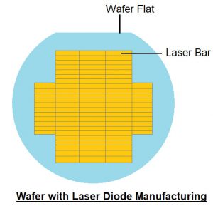
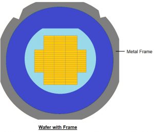
The wafers are placed on a sticky film such as blue tape, UV tape, or any type of flexible tape that attaches to the wafer while being easy to remove to make handling easier and avoid unexpected breakage. The metal frame is usually two inches larger in diameter than the wafer. All frame sizes and dimensions are according to international standards. This frame helps to hold the wafer during the Scribing and Breaking process. The metallic frames have specific features that make automated robotic handling easier, such as autoloaders. Frames fit properly in standard cassettes that carry a maximum of 25 frames.
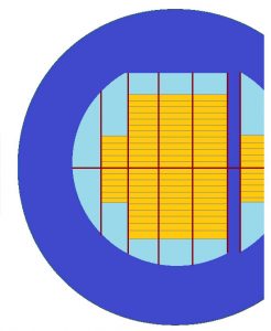
The wafer is then broken up into smaller portions that are easier to handle. To place the scribes along the wafer’s borders, a Laser Scriber or a Diamond Scriber is used. In an automatic tool, such as the Diamond Scriber, the wafer frame is placed on the machine, the appropriate processing program is selected, and the scriber automatically detects the structures and places the scribes in a moment. After the scribing process, the frame is removed from the scriber and the result can be seen in the below image.
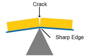
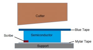
The below image is represented the side view of tape holding a wafer is bent over the sharp edge.
Following the placement of each segment on its frame, the frame is placed on the scribing tool. Different scribe lengths and patterns will be required depending on the material and scribing process. In the below image, a segment of the wafer is placed on a tape with a metal frame the scribes for the cell-to-bar process are set and the segment is cleaved into individual bars. The frame is removed from the scribing tool and placed in the breaker once the scribes have been placed.
A layer of Mylar tape is placed on top of the wafer to protect the devices that allow the breaker to perform their operation. After that, the wafer is placed on a breaking machine. The breaker takes over after selecting the accurate program and moves the wafer on top of the support. A camera positioned through the support ensures that the scribe is directly beneath the cutter. The wafer is struck from behind by the cutter, bending the semiconductor and cleaving the crystal along its planes. A continuous scribe is placed along almost the entire resonator length of the laser bar to ensure that all of the chips break. The frame can be moved to the breaker after the scribes have been fixed. Where the actual breaking operation will be performed automatically after the correct program is selected.
2.Saw Dicing:
Wafer dicing is also known as wafer sawing or wafer cutting. It is the act of separating a silicon wafer into separate components known as die or chips. Instead of performing a partial depth cut, the Saw Dicing procedure uses the cutting blade to completely saw through the wafer. Because the saw blade cuts through the full wafer width, mechanical sawing is also known as through cutting. The quality of the end product generated by mechanical sawing is determined by various criteria, including the cutting speed, blade thickness, blade size, and speed of the blade’s rotation. One disadvantage of thorough sawing is that the bottom side of the wafer may chip as a result of the blade cut. One method for reducing the danger of chipping is to put the wafer on a glass substrate. This can be done using specialty tape. These techniques can help prevent bottom-side chipping by providing additional support to the wafer during the dicing process.
The electronics and semiconductor industries have a substantial need for dicing saws, with a year-on-year increase in mass production and sales of various wafer dicing saw products around the world. In addition to typical applications in the semiconductor industry, use is increasing in the automotive and defense sectors. Increasing demand for semiconductor devices required for data centers and IoT, as well as an increase in self-driving cars and the component manufacturing industry, are some of the major factors to run the electronics and semiconductor industries. The product has a wide range of applications in power modules, MEMS, and sensors for the automotive, industrial, mobile, and medical markets. With semiconductors being used in practically every industry vertical, the market is expected to rise. Manufacturers are focused on reducing footprints while simultaneously expanding production capacity, thus sales are projected to grow throughout the course of the evaluation period. Nowadays Equipment’s manufacturers are focused on offering the world’s smallest fully automatic Dicing Saw equipment, setting new standards with their compact footprint, excellent efficiency, and creating even more prospects for growth in the region.
Wafer dicing permits integrated circuits and other semiconductor device manufacturers to harvest a large number of individual dice from a single wafer. The dicing process needs high-quality, high-precision machinery due to the exceedingly small size of the imprinted circuit traces on the wafer as well as careful monitoring by professional operators with the appropriate training and expertise. With the increasing popularity of high-density electronics, which is driven by the necessity to load more computing power into smaller containers, the wafer dicing process will continue to improve as semiconductor manufacturing techniques advance. There are various processes that can be performed using the standard functions in dicing saws.
- Full Cut Dicing Process
- Half-cut Dicing Process
- Dual-cut Dicing Process
- Step cut Dicing Process
Benefits of the Saw Dicing are mentioned below,
- Tooling is relatively low in cost.
- Low tool footprint
- Tool is much less complex as compared to Laser Dicing leading to shorter training times for tool operators.
- Well-known process.
Drawbacks of the Saw Dicing process,
- Mechanical stresses are applied to the wafer
- Die can fly-off from the tape during dicing
- Blade cost can be expensive
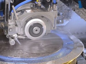
The below image of Dicing saw Equipment Disco DAD 321.

3. Laser Dicing:
Wafers are cut into small square or rectangular dies during the manufacturing of chips and microchips, a process known as wafer dicing. In wafer dicing applications, common issues include accurately positioning the cut, reducing material losses, and reducing component distortions. Simultaneously, the highest feasible machining speed must be accomplished. Laser dicing has become the dominant dicing technique as demand continues to grow. This non – contact laser method is flexible and prevents cutting-edge flaking. With different automated post-processing operations, the high quality of the edges, which is one of the critical criteria for fracture resistance, may be further increased. This eliminates manufacturing waste and, as a result, lowers production costs. As a result, laser-dicing procedures necessitate motion systems with excellent precision and straightness at high speeds. Laser dicing is a method of separating the silicon wafer into die using laser beam processes. Either feeding the laser over the front side of the thinned wafer or repeatedly irradiating the silicon wafer until a cut in the tape is made. Lasers have gradually replaced blade dicing for Si wafer dicing during the last decade. Laser systems are increasingly being used in the microelectronics industry for a variety of applications. Wafer cutting with a laser uses fewer consumables, is more closely focused, and is intended to result in less chipping. On the other hand, the laser ablation efficiency is determined by the energy interaction between the beam and the material. In other words, machining efficiency is determined by the laser type, which includes wavelength, pulse duration, beam shape, and material qualities such as thermal, mechanical, and optical properties.
Laser dicing has the potential to replace blade dicing as the next generation ultrathin wafer singulation technology because it allows for faster cutting, less damage, and a smaller kerf width, but a number of technical challenges must yet be overcome. The physics of laser-material interaction are addressed in terms of nanosecond, picosecond, and femtosecond pulse lengths for laser ablation and dicing of Si wafers. Increasing the feed speed with blade dicing has proven challenging. The Laser Cut Dicing is feasible to process at feed speeds 10 times quicker than blade dicing. Laser Dicing allows for a reduction in street width because the kerf width after processing is narrow and the kerf loss is lower when compared to blade dicing. Kerf is the width of material removed during the dicing process. Some compound semiconductor wafers, which include higher processing lines to singulate into the compact die, can raise the number of dies generated from a single wafer by reducing the street width.
The laser dicing is divided into two processes.
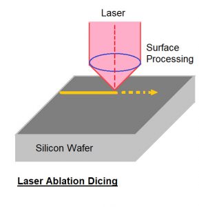
a) Laser Ablation Dicing:
A laser beam is focused onto the surface of the wafer at the desired place in the Laser Ablation Dicing. The laser energy is focused along with a cut pattern as needed to generate the cut through the wafer down to the bottom side of the wafer. Depending on the required beam intensity, a continuous wave laser is used to execute the dicing process. Cooling DI water is used to protect the wafer from thermal damage caused by the severe localized heating of the material by the laser. The cooling DI water also assists to eliminate any chopped particles and avoid contamination. There are three types of Ablation processes- grooving, scribing, and full-cut by adjusting the laser depth.
Grooving is the technique of removing the fine wire layer on the street’s surface using a non-contact laser and then cutting the residual substrate with blade dicing. This process reduces the problems like chipping, die cracking, and layer peeling.
Scribing is a process that involves creating a thin groove on the dicing street and then cutting the die by applying an external force, such as breaking.
In the Full cut process, high-quality processes without die cracking and chipping are possible using laser processing.
Because of the tendency of thinner wafers, the fragility of silicon is one of the major challenges when considering processing, such as cutting or scribing. Silicon separation is becoming increasingly significant in microtechnology and solar applications. As a result, non-contact procedures such as laser cutting by ablation techniques can be used, and research has been conducted to increase edge quality. The fundamental problem of using laser radiation to treat silicon is to avoid or limit damage and debris. Laser ablation is a procedure that melts or sublimates a portion of the silicon inside the material interaction zone. More heat is conducted into the bulk silicon as the contact time between the laser light and the lattice lengthens. The Laser ablation effect is affected by laser intensity and pulse duration. These characteristics also have a direct impact on cut quality and die strength, but further research is needed to examine the relationship. The breaking strength of silicon wafers cut with various laser sources, as well as their associated pulse durations and wavelengths, must be thoroughly investigated. Furthermore, utilizing the bending strength approach as the key parameter, a new cutting technique based on thermally controlled cracking will be examined and compared with different ablation processes. In the beginning, the ablation behavior of several laser sources with corresponding pulse duration and wavelengths is explored in order to establish process parameters for successfully cutting silicon samples. This is the foundation for demonstrating the strength of crystal silicon samples throughout various dicing techniques.
The features of Laser Ablation Dicing are listed below.
- Non-contact process with less load
- Low heat damage
- Enable the street width of less than 10um.
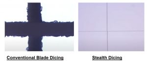
b) Stealth Dicing:
There is a trend in semiconductor fabrication to use huge wafers, even though the wafer itself is exceedingly thin. The dicing process poses a number of challenges such as how many chips can be diced from a single wafer or how to chop out chips of complex integrated circuits without generating flaws. Stealth Dicing Process is a technology that is vitally necessary for dealing with these tough conditions. This is one of the steps in the semiconductor production process where a modification in the dicing stage can have a significant impact on the entire process. However, the demands of the times necessitate the usage of tiny, high-performance semiconductor devices as the final semiconductor goods, which must be manufactured on thin wafers. The claim that market demands propelled Stealth Dicing Process to its current position in the semiconductor production industry is hardly exaggerated. With the introduction of stealth laser dicing, where micro damage is formed inside and propagates through numerous layers of this damage to eventually divide the wafer upon forced expansion through the tape, dry process singulation became possible without destroying the fragile components. On the other hand, it is based on infrared radiation, which is only visible and may penetrate through smooth surface silicon wafers at a specified resistivity or level of doping to create inner damage on the workpiece.
As a result, the stealth dicing method may struggle to handle Saw Street with metallization, strongly doped or high resistivity wafers, such as SOI wafers, and deep pits that may appear in some MEMS devices. This creates constraints on MEMS designs, processes, and material selection, which may extend beyond the active region to the dicing saw street. In terms of debris-free and entirely dry procedure, the Stealth Dicing method outperforms blade dicing as well as other laser dicing methods such as laser ablation. It is utilized to tackle numerous challenges in the dicing process, hence contributing to the creation of innovative devices and cost savings.
The Stealth Dicing technology was invented in Japan by Hamamatsu Photonics KK for dicing the ultrathin semiconductor wafers, but it has also performed successfully on silicon wafers of various thicknesses including specialty wafers with die attach films. Stealth dicing is an internal absorption laser process. A laser beam passes through the wafer and is focused beneath the surface. This process creates a modified layer in the workpiece by focusing a laser into the workpiece and then separating the die using a tape expander. This is a dry process that does not require any cleaning. Because the kerf width may be narrowed, it contributes to street reduction. There is no chipping or debris with stealth dicing, thus there is no need for a cleanup procedure. Because of its very narrow dicing route, it also decreases the number of wasted wafers, allowing for more chips and a greater manufacturing yield. This process does not cause heat damage, making the chips more resistant to breakage.
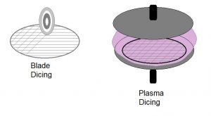
4. Plasma Dicing:
Plasma dicing is a high-quality invention that provides various advantages based on the end application. The ability to obtain a higher number of chips per wafer, as well as a reduction in process time, is critical in small chips, such as RFID tags, IoT devices, or MEMS sensors. The removal of contaminating particles is critical for devices such as image sensors, and the smoother, damage-free sidewalls with no heat-affected zones or cracking allow for an increase in the active area. The elimination of damage is crucial for memory IC designers. Increased processing time, High material loss due to the width of the dicing street, mechanical damage, and chipping are all new issues. To solve these concerns, a plasma dicing technology has been developed that, in some conditions, can replace mechanical dicing.
Plasma Dicing is also known as Deep Reactive Ion Etching. It is the dry etching process that etches narrow dicing streets into the wafer using a plasma gas such as Sulpher Hexafluoride. The procedure is performed throughout the wafer simultaneously, which means that all streets are etched at the same time, resulting in higher yields. The procedure can produce cuts that are non-rectangular in shape, which is not feasible with mechanical blade dicing. Plasma dicing causes minimal damage to the wafer surface or trench sidewall, resulting in better die strengths, improved device reliability, and longer device life. Plasma dicing delivers shorter cycle times and lower manufacturing costs as compared to mechanical dicing. There are various advantages of the Plasma Dicing process as given below,
1) All dicing streets are engraved at the same time, resulting in throughputs at least twice as fast as mechanical sawing.
2) The Plasma dicing, unlike saw dicing, does not damage the wafer surface, leading to higher die strength, device reliability, and device lifetime.
3) Plasma dicing’s Lower Street widths free up valuable wafer real estate, enabling a higher die count per wafer.
4) Non-rectangular die forms are also possible in Plasma Dicing.
The Plasma Dicing process has two methods.
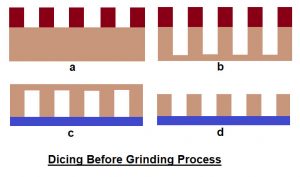
Dicing Before Grinding:
In this process, the streets are etched initially from the front side of the wafer to a depth of around 200 microns. Following that, the wafer is inverted and mounted to a dicing frame while a grinding mechanism thins off the wafer from the backside until the wafer is separated into die.
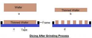
Dicing After Grinding:
The DAG method begins with wafer thinning, then connects the thinned wafer to a taped dicing frame and begins etching to form streets down to the tape. It is critical to avoid notching at the interface between the wafer and the tape since this can weaken the die more than physically sliced wafers.
You might also want to check out another article in our blog, which talks about the Dicing Process. Is there anything we can help you with? Contact us now to find out more