Bao bì khuôn nhúng: Hướng dẫn cơ bản
In this guide, we’ll delve into what exactly embedded die packaging is, exploring its definition, and the myriad of benefits it provides across various applications. From space-saving designs to improved heat dissipation, this innovative approach to integrating semiconductor dies is pivotal for modern electronics.
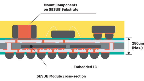
Image courtesy: ASE
With a comprehensive overview of the embedded die packaging market, including its size, key players, and market segmentation, as well as a dive into the latest technologies and advancements, this article will serve as your ultimate guide. Prepare to gain insight into the applications, challenges, and future trends shaping this transformative technology.
What is Embedded Die Packaging?
Embedded die packaging is a cutting-edge method where a semiconductor die is embedded within a layer of the printed circuit board (PCB) substrate rather than being mounted on the surface. This innovative approach is a deviation from traditional surface mount technology and chip-on-board techniques. It has emerged as a solution addressing the constant demand for miniaturization while enhancing electrical and thermal performance in electronic devices.
With technology spearheaded by industry leaders such as Taiwan Semiconductor Manufacturing Company and TDK Corporation, embedded die packaging paves the way for electronics design that is slim and more integrated than ever before. This packaging technology is being rapidly adopted by critical market segments, including consumer electronics, automotive sectors serviced by companies like Infineon Technologies AG, and telecommunications infrastructures across various regions from North America to the Middle East & Africa.
Benefits of Embedded Die Packaging
One of the most compelling benefits of embedded die packaging is improved size reduction, allowing the development of smaller, more compact electronic products without compromising functionality. This is essential for keeping pace with the stringent space constraints in modern device design.
Additionally, embedded die packaging offers enhanced thermal performance over traditional methods. Since the die is surrounded by substrate material, heat dissipation is significantly improved, which is critical for maintaining the reliability and longevity in high-power applications like those found in the automotive sector.
Electrical performance is also enhanced due to the short interconnections between the die and the substrate, which reduce parasitic inductance and capacitance, leading to faster signal transmission and reduced electrical noise.
Furthermore, because the die is protected within the substrate, embedded die packaging technology often results in increased product reliability and robustness – factors that are highly valued in market segments such as aerospace and medical devices, where stringent regulatory approvals are a norm.
Embedded die packaging is also a key player in enabling technological innovations. It aligns with the move towards more complex, multi-functional devices by allowing for greater integration of different components. This integration can facilitate the development of new and innovative form factors across various market segments, including automotive, telecommunications, and consumer electronics, which are continually pushed by companies such as Microsemi Corporation and Techuanikischer.
Lastly, with an increasing focus on efficiency and the need for high-speed electronic products, the adoption of embedded die packaging is projected to grow, making it a vital component of the global packaging market. It supports companies in achieving competitive advantages through product differentiation and upholds the market’s drive towards next-generation technological advancements.
Market Overview
The embedded die packaging market has been witnessing significant growth attributed to the demand for advanced packaging solutions across a myriad of sectors. This market is driven by the continuous evolution in electronic devices that require smaller form factors, higher performance, and greater functionality. Embedded die packaging technology responds to these needs by offering a superior alternative to traditional packaging methods, enabling manufacturers to produce more efficient and compact electronic products.
Advancements in the automotive sector, consumer electronics, and telecommunication infrastructures, particularly in regions like North America, South America, and the Middle East & Africa, are acting as catalysts for expansion in the embedded die packaging industry. Regulatory pressures for more environmentally friendly and efficient solutions also play a vital role in fostering innovation and adoption of embedded die packaging techniques.
Moreover, the shift towards wearable devices and the increased demand for flexible boards further fuel the industry’s growth, as embedded die packaging can deliver the required physical flexibility and performance. With its enhanced thermal and electrical performance and size reduction capabilities, embedded die packaging is expected to maintain its trajectory of growth, making it an essential aspect of the electronics packaging market.
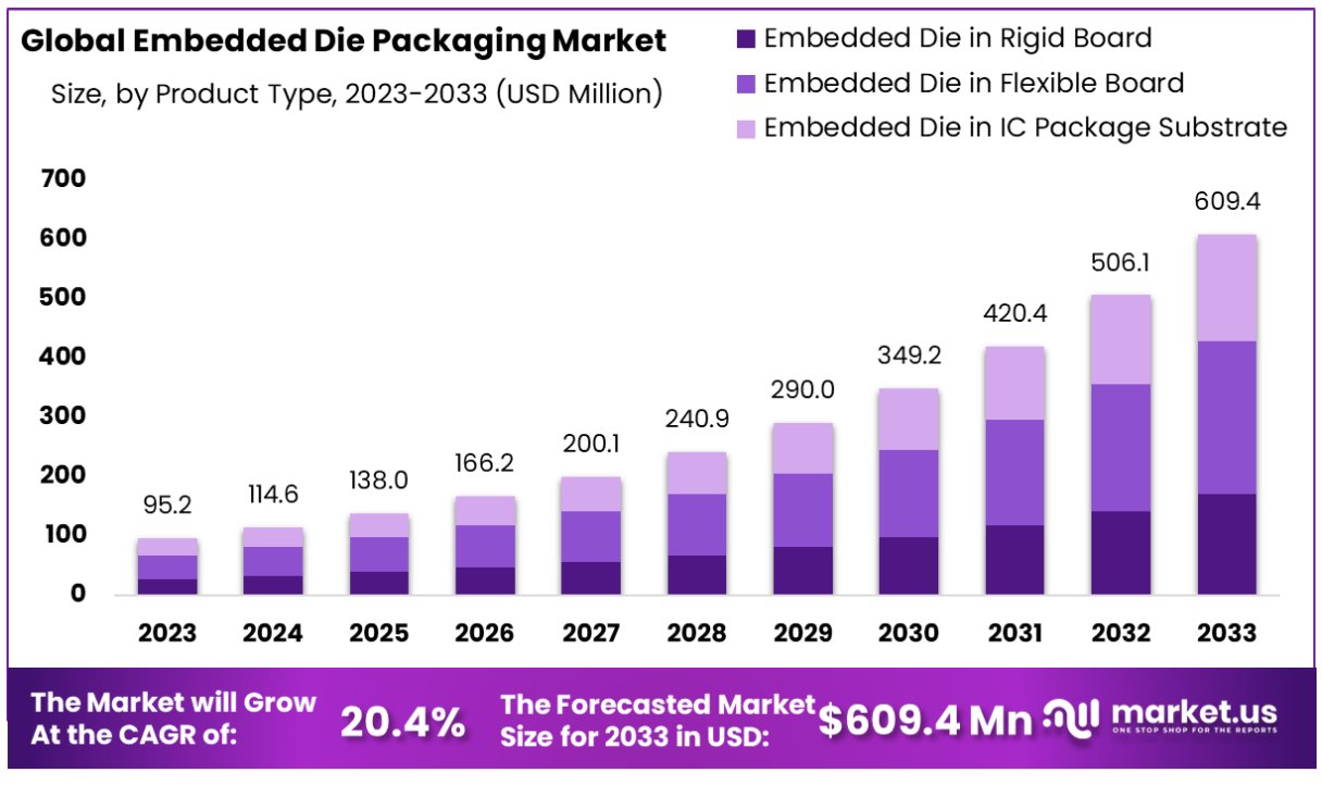
Global Embedded Die Packaging Market Size and Growth
The global embedded die packaging market is projected to expand significantly over the next few years. Market intelligence suggests an upward trend, with substantial annual growth rates driven by technological innovation and growing market demands. In regions such as Asia-Pacific, led by technological hubs like Taiwan and South Korea, the adoption of advanced packaging technologies, including embedded die solutions, is particularly robust.
Size reduction and the integration of multiple functions into single package substrates are key factors propelling the market forward. With the proliferation of electronic products requiring complex, yet small-sized, solutions, the ability of embedded die packaging to meet these requirements sets the pace for its market growth. Outside of Asia-Pacific, markets in North America, Europe, and other developing regions are also expanding, as economies seek the benefits of enhanced electronic components.
Key Players in the Embedded Die Packaging Market
The embedded die packaging market comprises a competitive landscape with several influential entities shaping its dynamics. Prominent amongst these is the Taiwan Semiconductor Manufacturing Company, a leading force in semiconductor manufacturing. Other key players, including TDK Corporation, Infineon Technologies AG, and Fujikura Ltd., drive the market with their innovative solutions and technological prowess.
In addition to these, Microsemi Corporation, Schweizer Electronic AG, and other entities serve important roles within the market. These companies consistently upgrade their offerings and invest in R&D to stay ahead of the curve in embedded die packaging techniques, ensuring they meet evolving demands in the electronic components market.
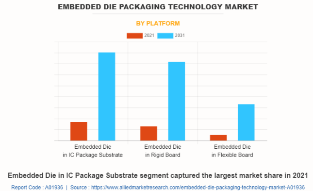
Market Segmentation
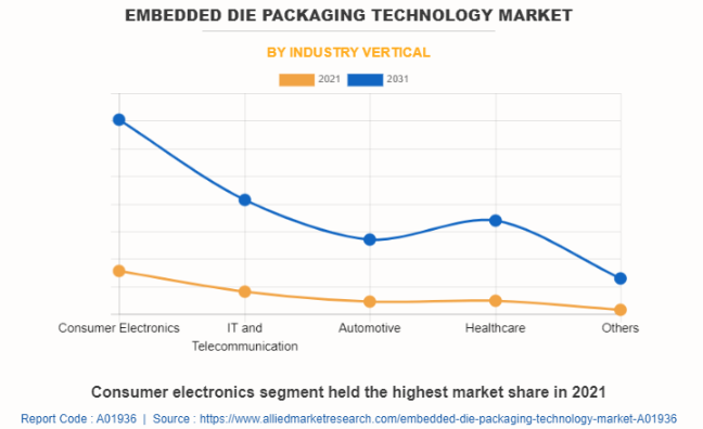
The market segmentation for embedded die packaging can be analyzed from several angles, including application, region, and end-user industry. Some of the main sectors are Consumer Electronics, where the need for compact and efficient packaging is paramount, and the Automotive sector, which requires robust and high-performance components.
Geographically, the embedded die packaging market is dissected into key regions such as North America, Europe, Asia-Pacific, the Middle East & Africa, and South America, each demonstrating unique growth patterns and contributing to the overall market size. Furthermore, the market is categorized based on technology type and the nature of applications such as smartphones, wearable devices, medical equipment, and aerospace components, which have distinct requirements necessitating the benefits offered by embedded die packaging solutions.
Technologies and Advancements in Embedded Die Packaging
Embedded die packaging technology stands at the forefront of semiconductor advancements, showcasing remarkable improvements in performance, miniaturization, and system integration. Key developments in this domain include the emergence of cutting-edge techniques for embedding dies within substrates, enhancing both the electrical and thermal performance of electronic modules. These advancements not only ensure a reduction in size but also improve reliability and offer better protection for the die.
Further, with the ongoing progress in material science, manufacturers have started utilizing high-density interconnect (HDI) substrates that allow for finer line spacing, and the incorporation of active and passive components into a single substrate. This technological innovation plays a crucial role in supporting the complex circuitry required by modern consumer electronics, automotive systems, and telecommunications equipment.
Another pivotal advance in embedded die packaging is the implementation of 3D packaging technologies. This approach stacks multiple dies vertically, as opposed to traditional side-by-side placement, significantly saving space and reducing interconnect lengths. The result is faster signal transmission and reduced power consumption, critical aspects in today’s high-speed electronic applications.
Advanced Semiconductor Engineering (ASE) Technology Holding
Advanced Semiconductor Engineering (ASE) Technology Holding is a global leader in semiconductor manufacturing and a pivotal player in embedded die packaging technology. ASE has been instrumental in developing integrated solutions that combine advanced package substriles with their expertise in chip packaging. Their approach to embedded die technologies emphasizes not only on size reduction but also on increasing functionality and improving thermal management.
ASE’s embedded die packaging solutions are geared towards enabling high-density integrated circuits within a compact footprint, which is particularly beneficial for applications such as wearable technology, mobile devices, and high-performance computing. With a commitment to continual innovation, ASE continues to refine its technologies to meet the burgeoning demands of sophisticated electronic products.
Infineon Technologies AG
Infineon Technologies AG has set high benchmarks in the semiconductor industry with its impressive portfolio of embedded die packaging solutions. Infineon’s approach largely focuses on enhancing the power density and efficiency of electronic components, which is crucial for automotive, industrial, and power management applications. Their packaging solutions are designed to withstand harsh environments, delivering reliability and longevity — attributes highly valued in these sectors.
Emphasizing robustness, their embedded die packaging technologies cater to high reliability applications, integrating enhanced protective features for the chips. Infineon’s advances in the encapsulation process and substrate development ensure that embedded components meet the stringent quality and durability standards required, particularly in automotive and industrial settings.
Amkor Technology Inc.
Amkor Technology Inc. is another key figure in the embedded die packaging landscape, renowned for its extensive service offerings that cover a wide spectrum of packaging needs. Amkor’s embedded die packaging capabilities are at the edge of the technology curve, facilitating size reduction and performance boost for a slew of electronic devices.
Leveraging advanced substrate technologies and a deep understanding of system-level integration, Amkor provides embedded die solutions that align with the trending demands for smaller, faster, and more efficient components. As technological advancements continue to evolve, Amkor invests in research and development to stay competitive, ensuring their offerings meet the high standards of the ever-changing electronics industry.
Applications of Embedded Die Packaging
Embedded die packaging has carved out a strong niche in various market segments, where its immense value in size reduction, improved performance, and enhanced reliability is widely recognized. This technology revolutionizes traditional electronic devices by embedding semiconductors directly into the package substrate. Across North America, South America, and the Middle East & Africa, key players like Infineon Technologies AG and TDK Corporation continually refine embedded die technology, tailoring it to the specific needs of diverse industries such as automotive, consumer electronics, medical, and telecommunications.
Automotive Industry
In the automotive sector, the demand for advanced electronic components is perpetually rising, driven by the evolution of electric vehicles (EVs) and autonomous systems. Embedded die packaging is a key enabler in this transformation, allowing for greater power density and reliability under extreme operating conditions—a specialty of companies like Infineon Technologies AG. With the ability to withstand high temperatures and vibrations, these packages ensure long-term durability and performance critical for safety-critical automotive applications. Embedded die technology also contributes to more compact modules, essential in vehicles where space is at a premium.
Consumer Electronics Industry
The world of consumer electronics is another domain significantly impacted by embedded die packaging. The overarching drive for smaller, lighter, and more powerful devices aligns perfectly with the capabilities of this packaging technique. From wearable devices to smartphones, embedded die packaging facilitates the slim form factors and sleek designs that consumers crave. Market leaders like TDK Corporation and Fujikura Ltd. push the envelope in integrating the technology into flexible boards, enhancing both the aesthetic and functional aspects of various gadgets.
Medical Applications
Embedded die packaging is making waves within the medical sector by enabling the development of compact, high-performance devices essential for patient care and monitoring. These robust packages can be found in implantable devices, portable diagnostics, and other medical equipment where size and reliability are paramount. Advanced substrate technology ensures these devices adhere to stringent regulatory approvals and meet the healthcare industry’s demands for durability and precision.
Telecommunications Industry
In telecommunications, the role of embedded die packaging is underscored by the increasing need for advanced infrastructure to support the growing data traffic and evolving wireless standards. Companies like Microsemi Corporation and Schweizer Electronic AG deliver solutions that boost electrical performance and signal integrity in equipment such as routers, switches, and base stations. By improving thermal management and reducing electromagnetic interference, embedded die packaging proves critical for reliable, high-speed communication networks.
Embedded die packaging stands as a transformative force across these industries, promising ongoing innovation as it adapts to the changing landscapes of electronic products and their applications. With market size expansion in regions including Saudi Arabia and South Africa, this technology’s contribution to various sectors looks set to climb, powered by the technological advancements and diverse form factors embedded die packaging can support.
Challenges and Trends in Embedded Die Packaging
Embedded die packaging technology must constantly evolve to meet the changing demands of the electronics industry. One of the key challenges it faces is balancing the drive for miniaturization with the need for high performance and reliability. As electronic devices shrink in size, the space available for components becomes increasingly limited, pushing packaging technologies to innovate.
Another trend is the demand for enhanced thermal and electrical performance. Embedded die packaging must dissipate heat effectively and ensure signal integrity to sustain the high performance of advanced electronic devices. Additionally, supply chain complexities, maintaining consistency in quality, achieving cost-effectiveness without compromising on performance, and navigating varied regional market conditions present ongoing challenges.
Increasing Demand for Compact and High-Performance Devices
The consumer electronics market exemplifies the demand for smaller devices with high-speed functionality. Embedded die packaging enables the integration of multiple functions within a compact space, satisfying consumer preferences for sleek and portable devices. In the automotive industry, the trend toward electrification and autonomous driving systems necessitates components that occupy less space but offer greater functionality and resilience.
Technological Advancements in Packaging Technology
Recent technological advancements are propelling embedded die packaging forward. Innovations in substrate materials and die attachment techniques have improved thermal and electrical performance. Developments such as three-dimensional (3D) packaging further maximize space efficiency and performance. Key industry players, including Taiwan Semiconductor Manufacturing Company and Fujikura Ltd., focus on enhancing integration capabilities and increasing the number of I/O ports without inflating size.
Growing Adoption of Embedded Die Packaging in Various Industries
There is a growing trend of embedded die packaging adoption across multiple industries beyond consumer electronics and automotive – such as in medical devices, aerospace, and telecommunications. In these sectors, embedded die packaging supports the creation of devices that are not only more functional and reliable but also comply with industry-specific standards and requirements, such as those found in life-critical healthcare applications or harsh aerospace environments.
Regulatory Approvals and Compliance Challenges
As embedded die packaging finds applications in sensitive industries, manufacturers must navigate a maze of regulatory approvals and compliance standards. This is especially true in the healthcare and automotive sectors, where patient and user safety are paramount. Achieving and maintaining certifications can be an intricate and time-consuming process, and companies must ensure that their products meet the regulatory requirements of each market they serve, ranging from North America to South America, and from Europe to the Middle East & Africa.
Regional Analysis of Embedded Die Packaging
The embedded die packaging market is witnessing significant growth around the world. With advancements in electronic device technologies and the increasing need for miniaturized components, the demand for embedded die packaging solutions is expanding across various regions, tailoring to their unique industry needs and market dynamics.
North America
North America is a prominent market for embedded die packaging, largely supported by the high demand for advanced electronic devices and the presence of key industry players in the region. The market is characterized by a strong emphasis on technological innovation and a robust telecommunications and consumer electronics sector. Companies in the United States and Canada are focusing on enhancing the capabilities of wearable and portable devices, driving the need for space-efficient packaging solutions. Regulatory approvals often drive the adoption of new packaging technologies, ensuring devices meet stringent performance standards.
Europe
Europe’s embedded die packaging market is driven by the automotive sector and technological advancements in electronic products. European manufacturers like Infineon Technologies AG are at the forefront of integrating embedded die technology for automotive electronics, catering to the demand for smaller, more efficient components within vehicles. Europe’s stringent regulations and high standards for electronic devices further dictate the need for high-quality embedded die packaging solutions that can withstand demanding environments and ensure reliability.
Asia Pacific
The Asia Pacific region is a rapidly growing market for embedded die packaging, with key players such as Taiwan Semiconductor Manufacturing Company and Fujikura Ltd. leading the way. Technological innovation and a large consumer electronics base fuel market growth. The presence of dense manufacturing hubs and advancements in electronic technology contribute to the Asia Pacific’s dominant position in the market. Flexibility in form factors and the push for size reduction in electronic devices, particularly in countries like South Korea and Japan, contribute significantly to the expansion of the embedded die packaging industry.
Latin America
In Latin America, there is a growing interest in embedded die packaging driven by the rising consumption of electronic products. Although the market size is smaller when compared to other regions, countries such as Brazil and Argentina are increasingly adopting modern electronic devices that necessitate advanced packaging technologies. The region shows potential for growth as local manufacturers aim to improve electrical and thermal performance in consumer electronics and telecommunications segments.
Middle East and Africa
The Middle East and Africa (MEA) region, while still an emerging market for embedded die packaging, is experiencing growth due to increased demand for consumer electronics and growth in the telecommunications sector. Countries like Saudi Arabia are investing in technological infrastructure, which could lead to greater adoption of sophisticated electronic devices. Although the market is challenged by the need for regulatory approvals and certifications, there is a significant opportunity for embedded die packaging solutions to address the needs of a diversifying electronic market in the MEA region.
Future Outlook for Embedded Die Packaging
Embedded die packaging technology, often utilized in electronic devices for its space-saving benefits, is poised for growth with advancements in areas like automotive and consumer electronics driving demand. As a critical component in modern electronic product design, key players including TDK Corporation, Infineon Technologies AG, and Taiwan Semiconductor Manufacturing Company are actively pushing the boundaries of form factors and package substrate innovations.
The market’s future outlook indicates expansion, with North America and emerging techno-hubs like South Africa and the Middle East & Africa set to play pivotal roles. Growth within these regions can be attributed to advancements in telecommunications and the burgeoning automotive sector, particularly in nations such as Saudi Arabia.
Technological innovation continually refines thermal and electrical performance, aiding market segments like wearable devices to benefit from embedded die packaging’s size reduction capabilities. Regulatory approvals also shape the landscape, ensuring the safe integration of this technology in various applications.
A concise list of factors influencing the future of embedded discover packaging is:
- Technological advancements in electronic products.
- Increase in demand for compact and flexible boards.
- Expansion in automotive and telecommunications sectors.
- Strong market presence of key players including TDK Corporation and Infineon Technologies AG.
- Growth in market segments like wearable devices.
The forecasted market size suggests a significant upswing, with South America also emerging as a vital contributor to the packaging market. Technological innovations and a focus on better-performing electronic devices will catalyze industry enhancements, benefitting both manufacturers and consumers alike.