Vượt qua những thách thức xác minh của SPI NAND Flash Octal DDR
As the automotive industry continues to evolve, the demands for high-capacity, high-speed storage solutions are intensifying. Autonomous vehicles and V2X (Vehicle-to-Everything) communication systems generate and process massive amounts of data, necessitating advanced storage technologies capable of meeting these demands. NAND Flash memory, particularly in its Serial NAND form, has emerged as a critical component in this space, offering higher memory density compared to alternatives like NOR Flash. However, the adoption of new architectures, especially those involving SPI Octal DDR interfaces, presents unique challenges in the verification of these storage solutions.
Durlov Khan, a Product Engineering Lead at Cadence, gave a talk at the FMS 2024 Conference, on how his company helped overcome these verification challenges.
Challenges in Verifying SPI NAND Flash Octal DDR
One of the significant hurdles in integrating SPI Octal DDR NAND Flash into automotive applications is the difficulty in accurately verifying these advanced storage devices. Traditional verification models for NOR Flash memory cannot adequately model the architecture and addressing schemes of Serial NAND Flash memory, especially when it comes to the Command-Address-Data (C-A-D) instruction sequences.
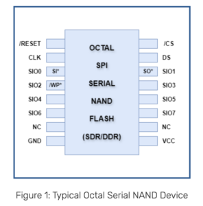
Existing models for x1, x2, or x4 SPI Quad NAND devices fall short in simulating Octal SPI NAND devices due to key differences in architecture. Octal SPI NAND uses an 8-bit wide data bus, requiring more complex Command-Address-Data (C-A-D) sequences and additional signal pins (SIO3-SIO7), which aren’t supported by Quad SPI models.

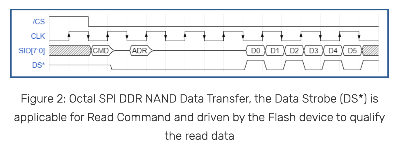
Additionally, Octal devices operate at higher frequencies with stricter timing parameters, including the use of a Data Strobe (DS) signal for data synchronization. These factors make existing Quad SPI models inadequate for accurately simulating the behavior of Octal SPI NAND devices.
Attempting to replicate an Octal device by combining multiple SPI or SPI Quad NAND devices is not feasible due to signaling incompatibilities and significant discrepancies in AC/Timing parameters, leading to inaccurate verification results. This gap in verification capabilities poses a substantial risk, as it limits developers’ ability to ensure that their automotive storage solutions will perform reliably in real-world scenarios.
Collaborative Solution: SPI NAND Flash Memory Model Enhancement
To address these challenges, a collaborative effort was undertaken by Cadence, in partnership with Winbond, leading to the development of a robust solution for SPI Octal DDR verification. This solution centers around the enhancement of the Cadence SPI NAND Flash Memory Model, which now supports the new SPI Octal DDR capabilities.
This enhanced Memory Model can be activated through a configuration parameter and includes additional support for a Volatile Configuration Register. This register allows users to program the correct Octal transfer mode, enabling accurate simulation of the SPI Octal DDR interface. In this mode, legacy SI and SO pins are repurposed, and new SIO3-SIO7 pins are introduced, along with a Data Strobe (DS) output pin that works with read data to signal the host controller at maximum DDR frequencies.

The model is fully backward compatible and can operate in multiple modes, including 1-bit SPI Single Data Rate (SDR), 1-bit SPI Double Data Rate (DDR), 8-bit Octal SPI SDR, and 8-bit Octal SPI DDR, depending on user configuration. This flexibility ensures that developers can accurately simulate a wide range of operational scenarios, crucial for the varying demands of automotive applications.
Real-World Application and Results at NXP
The integration of the Cadence VIP into NXP’s test environment demonstrated the effectiveness of this solution. The VIP seamlessly supported various density grades of SPI NAND Flash, with commands automatically adapting to the specific density grade in use. This adaptability and the ability to accurately model the SPI Octal DDR interface provided NXP with a reliable verification tool, ensuring that their storage solutions met the stringent performance and reliability standards required in the automotive sector.
Summary
The challenges in verifying SPI NAND Flash Octal DDR devices highlight the complexities of developing advanced storage solutions for the automotive industry. However, through collaborative efforts and innovative solutions like the enhanced SPI NAND Flash Memory Model from Cadence, developers can overcome these challenges. This advancement not only supports the current needs of automotive applications but also lays the groundwork for future innovations in storage technology, ensuring that the next generation of vehicles can handle the ever-increasing demands of data processing and storage with efficiency, reliability, and security.
For more details, visit Cadence’s SPI NAND solutions page.
Also Read:
The Impact of UCIe on Chiplet Design: Lowering Barriers and Driving Innovation
The Future of Logic Equivalence Checking
Theorem Proving for Multipliers. Innovation in Verification
Share this post via:


