TSMC công bố công nghệ logic tiên tiến nhất thế giới tại IEDM
Key Takeaways
- TSMC unveiled its 2nm Platform Technology featuring energy-efficient gate-all-around (GAA) nanosheet transistors for AI, HPC, and mobile applications.
- The N2 technology achieves a 15% speed gain or 30% power reduction compared to the 3nm node, showing over 140x energy efficiency improvements since the 28nm node.
- Currently in risk production, N2 is scheduled for mass production in the second half of 2025, with a faster 5% enhanced version, N2P, aimed for 2026.

There was a lot of discussion at IEDM about the coming shift to gate-all-around (GAA) transistor structures. This new device brings many benefits to continue device scaling, both at the monolithic device level as well as for multi-die design. The path to GAA is not simple, there are new material, process and design considerations to tame. TSMC has devoted a substantial amount of effort here. Let’s look at some of the details disclosed when TSMC unveils the world’s most advanced logic technology at IEDM.
About the Presenter

Dr. Geoffrey Yeap presented 2nm Platform Technology featuring Energy-efficient Nanosheet Transistors and Interconnects co-optimized with 3DIC for AI, HPC and Mobile SoC Applications on Monday at IEDM. He is Vice President, TSMC R&D Advanced Technology. Geoffrey has been at TSMC for almost nine years and has also led advanced work at Qualcomm, Motorola Mobility, AMD, and the University of Texas System Center for Supercomputing.
Geoffrey explained that the work he was presenting spanned four years and involved many staff members in TSMC’s Global R&D Center.
Presentation Overview
According to the IEDM press kit, this late news paper presents the world’s most advanced logic technology. As the title says, the work is focused on a leading edge 2nm CMOS platform technology (N2) that has been developed and engineered for energy-efficient compute in AI, mobile and HPC applications. Geoffrey explained that since the generative AI break-through in Q1’23, AI together with 5G-advanced mobile and HPC have created a huge appetite in the semiconductor industry for best-in-class energy-efficient logic technology and this work responds to that need.
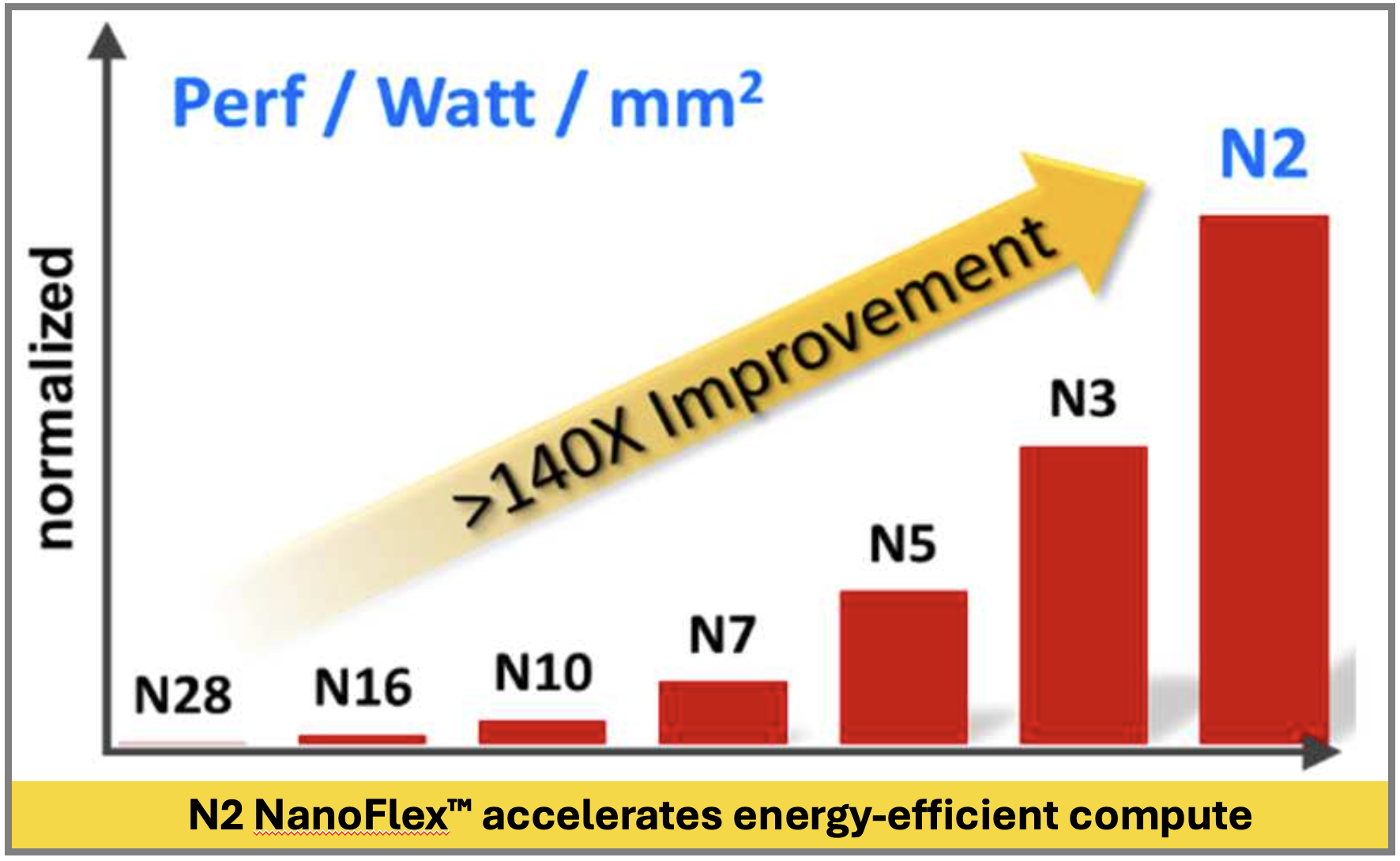
Geoffrey described the state-of-art TSMC N2 technology and its successful transition into NS platform technology with acceleration of >140x energy-efficient compute from 28nm to N2, as depicted in the graphic at the top of this post. The N2 logic technology features energy-efficient gate-all-around nanosheet transistors, middle-of-line and backend-of-line interconnects with the densest SRAM macro of ~38Mb/mm2. N2 delivers a full node benefit from the previous 3nm node in offering 15% speed gain or 30% power reduction with >1.15x chip density increase.
The N2 platform technology is equipped with new copper scalable RDL interconnect, flat passivation and TSVs. It co-optimizes holistically with TSMC’s 3DFabric™ technology enabling system integration/scaling for the target AI/mobile/HPC product designs.
Geoffrey reported that N2 has successfully met wafer-level reliability requirements and passed 1,000 hours of HTOL qualification with high yielding 256Mb HC/HD SRAM, and logic test chip (>3B gates) consisting of CPU/GPU/ SoC blocks. N2 is currently in risk production. N2 platform technology is scheduled for mass production in the second half of 2025. N2P, a 5% speed enhanced version of N2 with full GDS compatibility, is targeted to complete qualification in 2025 and go to mass production in 2026.
Some More Details
From a platform perspective, Geoffrey provided some details about the N2 NanoFlex™ technology architecture. System technology co-optimization (STCO) was utilized with smart scaling features rather than brute-force design rule scaling which can drastically increase process cost and inadvertently causes critical yield issues. Extensive STCO coupled with smart scaling of major design rules (e.g., gate, nanosheet, MoL, Cu RDL, passivation, TSVs) was performed in optimizing the technology to achieve the target PPA.
He pointed out that co-optimization with 3DFabric SoIC 3D-stacking and advanced packaging technology (INFO/CoWoS variants) was done, thereby accelerating system integration/scaling for AI/mobile/HPC product designs. N2 NanoFlex standard cell innovation offers not only nanosheet width modulation but also a much-desired design flexibility of a multi-cell architecture.
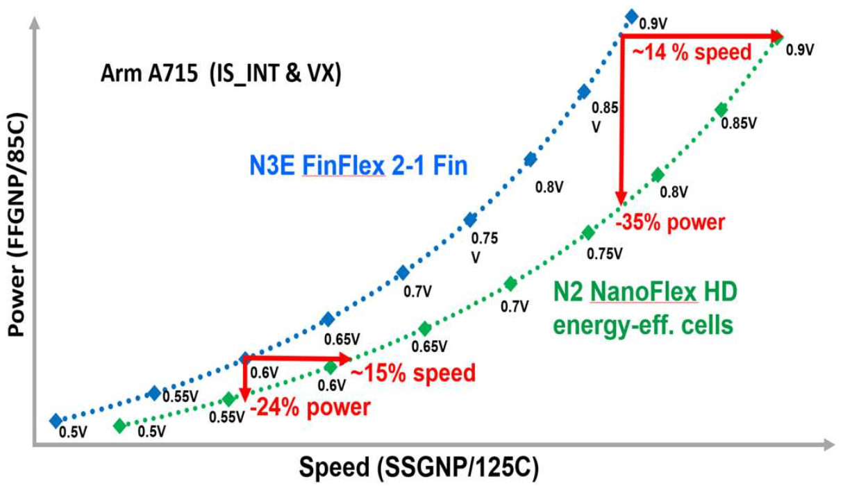
This capability delivers N2 short cell libraries for area and power efficiency. He explained that selective use of tall cell library elements lifts the frequency to meet design targets. With six Vt offerings spanning 200mV, N2 provides unprecedented design flexibility to satisfy a wide spectrum of energy-efficient compute applications at the best logic density. The figure below illustrates some of the benefits of this approach for an Arm-based design.

Geoffrey explained that N2 nanosheet technology exhibits substantially better performance/Watt than FinFET at the low Vdd range of 0.5V- 0.6V. Emphasis is placed on low Vdd performance/Watt uplift through process and device continuous improvements resulting in a 20% speed gain and 75% lower stand-by power at 0.5V operation. N2 NanoFlex coupled with multi-Vt provides unprecedented design flexibility to satisfy a wide spectrum of energy-efficient compute applications at the most competitive logic density.
Geoffrey went into more details on the SRAM, logic test chip and qualification and reliability. This was an impressive presentation. The N2 technology platform brings a lot of new capability to the table for future innovation. And that’s some of the details about how TSMC unveils the world’s most advanced logic technology at IEDM.
Share this post via:

