Thinking Small To Think Big: AMD Modular Architecture Is Advancing Sustainability – CSRwire.com
Now Reading
By: Justin Murrill, Director of Corporate Responsibility at AMD
By: Justin Murrill, Director of Corporate Responsibility at AMD
Published 04-23-24
Submitted by AMD
Tackling macro technology challenges often entails devising micro solutions that scale. At AMD, we have embraced this approach for 55 years as we design high performance and adaptive computing solutions. In my role to advance sustainability at AMD, I have seen incredible innovations where AMDers think small to think big and in doing so, create major co-benefits for technology users and the planet.
A powerful example is AMD developing “chiplets” – a revolutionary semiconductor design approach that embraces modular architecture. The innovation addresses several technology and sustainability challenges simultaneously such as cutting manufacturing environmental impacts and costs while increasing compute performance and energy efficiency. Instead of one large monolithic chip, AMD engineers reconfigured the component IP building blocks using a flexible, scalable connectivity we designed known as Infinity Fabric. This laid the foundation for our Infinity Architecture configuring multiple individual chiplets to scale compute cores in countless designs that further optimize energy efficiency.
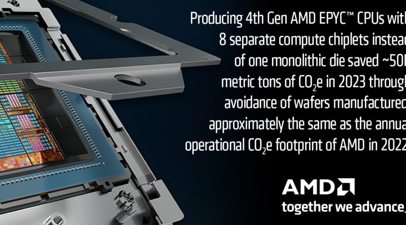
AMD recently measured the sustainability benefits of chiplets in the wafer manufacturing process for one product line, and the results are compelling. Producing 4th Gen EPYC CPUs with 8 separate compute chiplets instead of one monolithic die saved ~50K metric tons of CO2e in 2023 through avoidance of wafers manufactured, approximately the same as the annual operational CO2e footprint of AMD in 2022.i
Modular designs inherently provide sustainability benefits by leveraging interchangeable component configurations to provide flexibility in product offerings while cutting manufacturing cost and waste. For example, modular home construction is estimated to reduce waste by over 80% and cut costs nearly in half compared to a traditional new construction home.ii
In the case of the AMD modular chiplet approach, the waste reduced is the percentage of silicon wafers with defects. The silicon wafers are circular (300 mm diameter), and the individual chips are squares/rectangles. Each wafer is cut to yield a certain number of chips, and not all of them are perfect. The smaller the area of the chip, the more chips we can get per wafer and the lower the probability that a defect will land on any one chip. As a result, the number and yield percentage of “good” chips per wafer goes up, and the wasted cost, raw materials, energy, emissions and water goes down.
Like any disruptive design approach, AMD chiplet technology encountered initial skepticism – both internally among AMD engineers and externally from the competition, as AMD CTO Mark Papermaster and Sam Naffziger, senior vice president and AMD Corporate Fellow, discussed in this AMD Advanced Insights podcast. But by diligently following the data and devising key solutions, like a lightweight and high-speed communication fabric, the compelling benefits in performance capability, configuration flexibility and energy efficiency prevailed. Today, much of the industry is trying to replicate the chiplet approach.
Chiplets not only avoid waste and conserve resources in manufacturing, but also in the data centers powering the digital services and experiences we use daily. Each chiplet houses multiple processor cores, and different chiplets can be added and even stacked in a package to create higher-performance and more energy efficient processors. Today, AMD EPYC processors power the most energy efficient x86 servers on the market.iii Using the most energy efficient servers means far fewer physical servers are needed to meet computing demands, which has a cascading effect of avoided environmental impacts – less raw materials, manufacturing, shipping, energy use and data center space. This is critical for companies needing to modernize data center infrastructure and increase compute capabilities while also aggressively pursuing sustainability goals. A case in point is Europe’s largest semiconductor company, STMicroelectronics. By upgrading their server processors to AMD EPYC, they slashed electricity consumption by 33% as part of their strategy to reach carbon neutrality by 2027, all while increasing compute performance.iv
When sustainability is built into design, it can avoid the need to manage waste on the back end. Our chiplet design approach is not only reducing the energy consumption and carbon emissions from end devices like servers and data centers, but also reducing waste and avoiding emissions in the supply chain.
To learn more about environmental sustainability at AMD, visit: https://www.amd.com/en/corporate/corporate-responsibility/environmental-sustainability.html
Footnotes
[i]AMD estimation based on defect density (defects per unit area on the wafer), chip area and n-factor (manufacturing complexity factor) to estimate number of avoided wafers in one year. Yield = (1 + A*D0)^(-n) where A is the chip area, D0 is the defect density and n is the complexity factor. The Area is known from our design. D0 is known based our manufacturing yield data and n is a number provided by a foundry partner for a given technology. The calculations are not meant to be precise since chip design can have a large influence on yield, but it estimates the area impact on yield. The carbon emission estimates of 49,934 mtCO2e were calculated by entering in the estimated number of 5 nm wafers saved in one year based on the TechInsights’ Semiconductor Manufacturing Carbon Model. Comparison to AMD corporate footprint is based on AMD reported scope 1 and 2 market-based GHG emissions in 2022, 50,198 mtCO2e.
[ii]https://www.mdpi.com/2075-5309/11/12/622
[iii]EPYC-028C: SPECpower_ssj® 2008, SPECrate®2017_int_energy_base, and SPECrate®2017_fp_energy_base based on results published on SPEC’s website as of 11/10/22. VMmark® server power-performance / server and storage power-performance (PPKW) based results published at https://www.vmware.com/products/vmmark/results3x.1.html?sort=score. The first 80 ranked SPECpower_ssj®2008 publications with the highest overall efficiency overall ssj_ops/W results were all powered by AMD EPYC processors. For SPECrate®2017 Integer (Energy Base), AMD EPYC CPUs power the first 11 top SPECrate®2017_int_energy_base performance/system W scores. For SPECrate®2017 Floating Point (Energy Base), AMD EPYC CPUs power the first 12 SPECrate®2017_fp_energy_base performance/system W scores. For VMmark® server power-performance (PPKW), have the top four results for 2- and 4-socket matched pair results outperforming all other socket results and for VMmark® server and storage power-performance (PPKW), have the top overall score. See https://www.amd.com/en/claims/epyc4#faq-EPYC-028C for the full list. More information about SPEC® is available at http://www.spec.org. SPEC, SPECrate, and SPECpower are registered trademarks of the Standard Performance Evaluation Corporation. VMmark is a registered trademark of VMware in the US or other countries.
[iv]https://www.amd.com/en/resources/case-studies/stmicroelectronics.html
About AMD
For more than 50 years AMD has driven innovation in high-performance computing, graphics and visualization technologies. Billions of people, leading Fortune 500 businesses and cutting-edge scientific research institutions around the world rely on AMD technology daily to improve how they live, work and play. AMD employees are focused on building leadership high-performance and adaptive products that push the boundaries of what is possible. For more information about how AMD is enabling today and inspiring tomorrow, visit the AMD (NASDAQ: AMD) website, blog, LinkedIn and Twitter pages.
More from AMD

