Thiết kế và quy trình điều chỉnh cho khâu EUV NA cao
By Kevin Lucas and James Ban
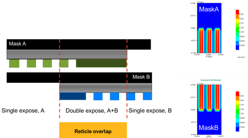
Upcoming 14A and 10A process nodes will use high-NA EUV anamorphic scanners, which will require two stitched half-fields to achieve the equivalent wafer exposure area of previous-generation scanners, see figure 1. The lithography patterning at a stitching boundary between two mask exposures will be affected by additional process variation than are encountered in single exposure patterning. Additional variations include exposure-to-exposure overlay/dose/focus offsets and mask-to-mask overlay/mask-CD offsets. These additional variations can be sufficiently large that patterns that printed with good control in single exposure regions on a chip can fail in the double exposure region. Thus, the allowed design patterns printed at a stitching boundary must be restricted (e.g. in width or in space) relative to patterns printed in single exposure regions.
Fig. 1: At left, a X-section view of the mask regions (main pattern, image border, black border) and the double exposure region in a stitched process. At right, a top-down view of the wafer intensity from each mask exposure for stitched line-end patterns which will ideally form three continuous lines on the wafer resist pattern.
Fortunately, there are a variety of different options for designing stitch-friendly target patterns, and for co-optimization of design & mask synthesis stitch-friendly lithography solutions. Options for design of stitch-friendly layout are shown in Table 1.
| Opportunities for design or process to enable high-NA EUV-friendly layout | Level in design-process flow |
| A. Reticle level floorplanning avoids odd # of chip rows | Reticle level |
| B. High level block placement ensures empty space at stitch region | Block level |
| C. Sub-block module placement provides extra space at stitch region | Module level |
| D. Custom std. cell or memory cell stitch-tolerant layout in stitch region, e.g., place only logic/memory cells which provide extra space between patterns | Cell level |
| E. Stitch-friendly rules or cost-functions avoid critical patterns in stitch region | Place & Route or stitching Design Rules |
| F. Stitch region-specific and stitch design rule-specific OPC/RET | OPC/RET |
Table 1: List of areas in the design-process flow where layout can be optimized to enable EUV-friendly layout.
Tight pitch routing metal with high-NA EUV
One of the most challenging patterning layers is the tightest pitch routing metal layers with expected minimum pitch of ~20nm for 1D metal lines with High-NA EUV. Rigorous simulations using Sentaurus Lithography (S-Litho) show that single exposure High-NA EUV can pattern 20nm pitch, single orientation lines with good CD control through expected process variations (e.g., 40-50nm DOF and 8-10% dose control).
However, imaging of 20nm pitch single orientation lines by stitching two mask exposures does not show sufficient CD control even with optimized OPC/RET due to additional process variations in the stitching region, see figure 2. Therefore, routing metal layouts must be more restricted in stitching regions. Unfortunately, as shown in figure 3, current metal routing designs often contain groups of minimum width and space lines where stitching would be needed.
Fig. 2: Example of S-Litho rigorous resist images from stitched line-end patterns as in figure 1. At best dose/focus/overlay (left) the line patterns resolve well, but not with expected process variations (right).
Fig. 3: Example of typical uni-directional tightest pitch metal routing in an advanced design with many groups of small, dense lines which will cross the stitch line of a chip and will cause patterning issues.
We tested different place & route (P&R) design optimizations using Fusion Compiler to reduce metal patterning issues, as measured by IC Validator design rule check (DRC) errors in the stitching region.
Figure 4 shows the routing congestion and stitching region DRC violations detected with:
- Testcase 1: a traditional P&R run (i.e., no high-NA optimization) which had 1365 DRC errors.
- Testcase 2: using “soft-blockage” P&R optimizations applied to reduce the density of patterns above and below the stitching region, which saw DRC errors reduced to 386.
- Testcase 3: with the P&R optimizations of test 2 and enabling P&R to create DRC-clean metal lines in the stitching region, which had only 10 DRC errors.
Overall, a 99% reduction in DRC errors was seen. Both max frequency and area of the final optimized design were found to be acceptable when compared to the reference design. These results show the potential for P&R optimization to ensure high-NA EUV friendly metal routing with minimal circuit impact.
- Testcase 1: Design w/o considering stitch region
- Testcase 2: Optimize placement modules and I/O ports including use of soft blockage
- Testcase 3: Testcase2 + allow M2~M4 routing inside stitch area w/ region-specific design rules
Fig. 4: Example showing P&R methods to reduce DRC errors in a 2um high stitching region of a layout block (shown at left). DRC errors are nearly all removed, and circuit frequency/area goals were achieved.
Although the design-based high-NA EUV optimizations drastically reduced the DRC errors, co-optimization with OPC/RET is still valuable. For example, a tuned OPC/RET flow (e.g., applying metal retargeting) enabled the stitch region specific design rules to be more aggressive and save circuit area. See figure 5 where S-Litho simulations show that the Proteus retargeted and OPC’d 1D stitched metal line-ends at a pitch of 26nm can be patterned well through expected process variations.
Fig. 5: Example of S-Litho rigorous simulations showing RET retargeting on stitched routing lines at looser pitch ensures high-NA EUV friendly layouts can print without wafer defects vs. expected process variations.
Conclusion
We have shown that allowed patterns printed at a stitching boundary must be restricted relative to the patterns printed at single exposure regions on the wafer. Therefore, the physical design of the chip must be aware of the stitching region and optimized to be stitching friendly. We have shown examples how high-NA EUV-aware P&R can avoid stitching unfriendly layout with low impact upon design goals, and that co-optimization of process and design tools and methods can benefit both patterning and circuit area for a high-NA friendly design.
James Ban is senior director of engineering, R&D, at Synopsys.
Kevin Lucas
Kevin Lucas is a senior architect for mask solutions products at Synopsys. He has expertise in OPC/RET, lithography design rule development, and lithography simulation. He has a Ph.D. in electrical engineering from Carnegie Mellon Univ. and is an SPIE Fellow.


