Semiconductor: China may have discovered a better chip material than silicon — here's what we know – Tech Wire Asia
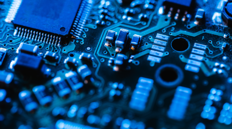
A robust recovery in semiconductor sales is forecasted, with an expected growth of 13.1% in 2024, as per the WSTS report. Photo: Shutterstock.
By Dashveenjit Kaur
Over a year after Gang Chen, a naturalized US citizen, was among dozens of scholars targeted by US authorities under the China Initiative, a controversial scheme launched under the Trump administration to root out espionage activities on campus. Following the dismissal of the case against Chen earlier this year, the professor of mechanical engineering at the MIT along with a handful of other researchers announced that they have discovered the “best semiconductor material ever found,” — and it may just be the best possible one.
For starters, Chen was arrested on January 14, 2021, during President Donald J. Trump’s last full week in office, and charged with omitting affiliations with Chinese government institutions in grant applications to the US Department of Energy in 2017. He pleaded not guilty to all the charges. The case against Chen, however, is the most prominent of the cases to be dismissed to date, involving an elite scientist who had robust support from his university.
Dashveenjit Kaur | 12 August, 2022
In essence, China-born Chen studies heat transfer and he has hopes to develop a semiconductor that could convert heat from car exhaust into electricity, or fabric for clothing that could cool the body. The year of his arrest, up till this year when the case against him were dismissed, Chen were torn away from proceeding with his research. The upside though, reuniting with his fellow researchers has allowed for the discovery of a material that apparently can perform much better than silicon.
The findings, first unveiled on Science Journal, were shared through a paper by MIT postdoc Jungwoo Shin and MIT professor of mechanical engineering Gang Chen; Zhifeng Ren at the University of Houston; and 14 others at MIT, the University of Houston, the University of Texas at Austin, and Boston College.
Silicon is one of the most plentiful elements on Earth, and in its pure form, the semiconductor material has become the foundation of much of modern technology, including microelectronic computer chips and solar cells. However, silicon’s properties as a semiconductor are actually far from ideal.
“For one thing, although silicon lets electrons whizz through its structure easily, it is much less accommodating to “holes” — electrons’ positively charged counterparts — and harnessing both is important for some kinds of chips. What’s more, silicon is not very good at conducting heat, which is why overheating issues and expensive cooling systems are common in computers,” Massachusetts Institute of Technology said in a news release.
That said, a team of researchers at MIT, the University of Houston, and other institutions has discovered what MIT calls the “best semiconductor material ever found,” which is even better than silicon. Basically, those researchers carried out experiments showing that a material known as cubic boron arsenide overcomes both of the limitations of silicon. It provides high mobility to both electrons and holes, and has excellent thermal conductivity.
It is, the researchers say, the best possible semiconductor found. “Heat is now a major bottleneck for many electronics,” said Jungwoo Shin, a postdoc at MIT and the lead author of the paper. He cited how silicon carbide, which has three times higher thermal conductivity than silicon, is replacing silicon in power electronics in electric vehicles, including those made by Tesla. The more advanced semiconductor compound saves weight and gives the vehicles a longer range.
“Imagine what boron arsenides can achieve, with 10 times higher thermal conductivity and much higher mobility than silicon,” he said, calling the material a potential “gamechanger.” Chen reckons that it is very attractive just for heat dissipation. The research also showed that the material has a very good bandgap, a property that gives it great potential as a semiconductor material.
Although cubic boron arsenide seems to tick all the boxes for an ideal semiconductor, it remains unknown whether it is a viable replacement for silicon as researchers have yet to find a practical way to produce quality cubic boron arsenide in bulk. “One major challenge is to grow high-quality cubic boron arsenide crystals,” Chen said. So far, researchers could only obtain crystals less than a centimeter in size, whose thermal and electrical properties are not uniform.
In another recent study, he also identified impurities that reduced the mobility of the material. “To commercialize this material, I think more effort is needed to investigate the synthesis of high-purity crystals,” Chen added. Until that is solved, if or how cubic boron arsenide can be applied is unclear, the study acknowledged. “Whether or where it’s going to actually be used, we do not know,” Chen noted.
So far, according to MIT, cubic boron arsenide has only been made and tested in small, lab-scale batches that are not uniform. The researchers had to use special methods originally developed by former MIT postdoc Bai Song to test small regions within the material. More work will be needed to determine whether cubic boron arsenide can be made in a practical, economical form, much less replace the ubiquitous silicon.
By Dashveenjit Kaur
![]() @DashveenjitK
@DashveenjitK
Dashveenjit Kaur | ![]() @DashveenjitK
@DashveenjitK
Dashveen writes for Tech Wire Asia and TechHQ, providing research-based commentary on the exciting world of technology in business. Previously, she reported on the ground of Malaysia’s fast-paced political arena and stock market.
© 2024 Tech Wire Asia | All Rights Reserved
Terms of use Privacy Policy


