Samsung Foundry Struggles with Yield and Power Efficiency Issues – BusinessKorea
This year, global fabless semiconductor and IT companies are expected to start adopting the 3nm process as their main fabrication method. It is anticipated that most companies will allocate their orders to TSMC, which is likely to widen the gap between TSMC and Samsung Electronics in market share.
As of June 17, industry sources report that seven companies including NVIDIA, AMD, Intel, Qualcomm, MediaTek, Apple, and Google have prioritized adopting TSMC’s 3nm process. It has been revealed that after considerable deliberation, Google and Qualcomm, which Samsung Electronics Foundry Division had long sought to secure as clients, have chosen TSMC.
Google's Tensor processor, up to its fourth generation, was entrusted to Samsung Electronics Foundry Division but starting with the fifth generation that introduces the 3nm process, it will utilize TSMC’s fabs. Last year, it was widely expected that the first batches of Qualcomm’s Snapdragon 8 Gen 4 would be outsourced to TSMC for production.
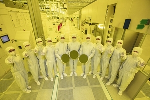
Despite declaring the start of 3nm process mass production three years ago, Samsung Electronics is facing difficulties in securing customers. In June 2022, it was the first in the industry to apply the 3nm gate-all-around (GAA) process to mass production. However, the first-generation 3nm node (SF3E) has been performing below expectations in yield and efficiency, finding adoption only in niche markets like cryptocurrency mining. Furthermore, the Exynos 2500, developed by Samsung System LSI Division and produced through Samsung Foundry's 3nm process, is also reported to have disappointing yields.
Industry experts cite poor yield and power efficiency as the main issues with Samsung Foundry’s 3nm process. In particular, Samsung Electronics is heavily focusing on controlling power consumption and heat, yet it still shows 10-20% lower performance compared to TSMC, according to analyses. With the expansion of AI services in mobile and server markets, chip power efficiency has become a critical factor.
A representative from a major global foundry company stated, “The main reason big customers choose TSMC is the difference in chip power efficiency offered by both companies at cutting-edge processes.” Despite TSMC raising the production costs for 3nm chips by more than 25% compared to 5nm, the choice for TSMC is due to the significant performance difference.
The representative also highlighted challenges in heat management. “Heat issues in semiconductors have been a longstanding challenge for leading chip manufacturers over the past 20 years, but it has become a crucial issue with the onset of the AI semiconductor era,” they explained. “In mobile chips, heat issues can compromise the entire structure of smartphones, and for server chips, the heat generated by one server rack can spread like wildfire, potentially causing overload across the entire server.”
The gap in the foundry market share between TSMC and Samsung Electronics is also growing. According to TrendForce, Samsung Electronics Foundry’s market share dropped slightly to 11% in the first quarter of this year from 11.3% in the last quarter of the previous year. Meanwhile, despite a decline in smartphone demand, TSMC saw its market share increase from 61.2% to 61.7% during the same period.
Additionally, starting from the 2nm process, Samsung Electronics aims to dramatically improve power efficiency issues with the introduction of Backside Power Delivery (BSPDN) technology, positioning it as a ‘game changer’ in the foundry industry. Initially planned for commercialization after 2027, Samsung has decided to expedite the adoption of this technology, aiming to start mass production of the 2nm process either next year or by 2026.
Never miss another article! Enter your email address below to receive our free daily newsletter:
