Quy trình Die Attach là gì?
Introduction:
Die Attach is also commonly known in the Semiconductor industry as Die Bonding or Die Mount. It is the process of attaching a silicon chip to the Die pad of the support structure, such as a leadframe or metal can header of the Semiconductor package. This is a critical step in the Semiconductor Backend manufacturing process and the use of specialized Die Attach/Die Bonding equipment is critical to ensure process productivity and quality.
Die Attach/Die Bonder machines such as ESEC 2008, Datacon 8800, Canon Bestem D511F, ASM 838/868 Die Bonders, and various precision Die Attach/Die Bonding tools are used to accurately Pick and Place the die onto the substrate.
Chips diced from a wafer are attached to the center pad of a substrate (Leadframe/header) called the die to attach pad with a variety of different available Die Attach processes:
1) Soft Solder Die Attach
2) Eutectic Die Attach
3) Epoxy Die Attach
4) UV Die Attach
5) Silver Sintering Die Attach
6) Thermocompression Die Bonding
7) Flip Chip Die Attach
What is the process of Die Attach?
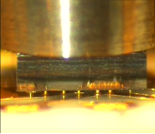
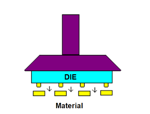
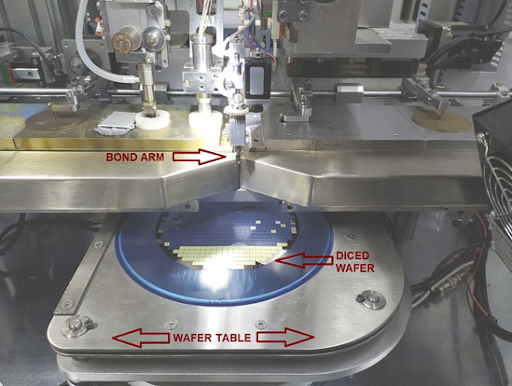
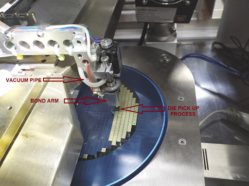
For the Die Attach/Die Bonding process, we align the position of the die and the substrate (leadframe) on the Die Attach/Die Bonding machine. The Pick Up Tool or Die Collet moves downwards (Z motion) either to the die surface or to a position just above the die. The Ejection tooling system consisting of Ejector Needles, Needle Holders and Pepper Pots on the machine coordinates the die ejection process together with the Pick-Up system to ensure that the die is successfully ejected and picked up from the adhesive film. Vacuum pressure holds the die during the transfer from the wafer to the leadframe/header.
Steps in Die Attach Process flow:
There are the following in the semiconductor Die Attach process:
- Wafer Expansion
- Die Attach/Die Bonding
Wafer Expansion:
Wafers (tested and probed) are obtained from wafer manufacturers. These wafers are sent for the wafer expansion process in which spacing between each die is enlarged, allowing more clearance between the die. The dies are maintained in their respective position of the wafer with clearance for pick up, optical recognition (Wafer Mapping), and Die bonding. The use of Wafer Expansion has reduced in recent times with the proliferation of smaller, thinner dies.
Die Attach/Die Bonding:
There are various Die Attach methods which are as follows:
1) Soft Solder Die Attach:
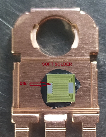
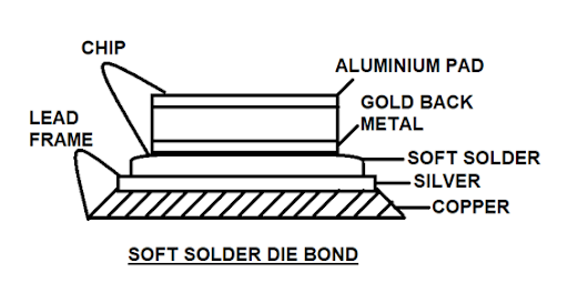
Soft Solder Die Attach process uses Soft Solder in wire roll form as Die Attach material to mount die on the Die Pad of the leadframe. The die is ejected from the wafer by ejector needles. While being ejected, a Pick and Place tool is commonly known as a Pick-Up Tool/Die Collet then retrieves the die from the wafer tape and positions it to the Die Attach area. Please refer to the diagram below:
2) Eutectic Die-Attach:
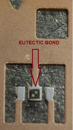
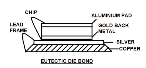
No Soft Solder preforms are used in the Eutectic Die Attach process. The leadframe in the bonding area is plated with silver (in selected areas and not in the entire lead frame). The backside of the die is usually plated with gold plating. Gold-silicon eutectic bonding is accomplished by placing the chip on the Die Attach pad of the lead frame and heating above the melting temperature of the Eutectic bond on the Eutectic Die Attach machine/Die Bonder. This forms a rigid joint between the lead frame and silicon. To facilitate die attachment scrub motion is used to initiate the Eutectic flow and force out air-pockets that may be present during the attachment process. See the below diagram eutectic attach on lead frame:
3) Epoxy Die-attach:
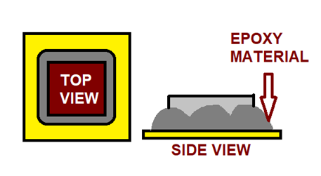
An Epoxy Die Attach process is performed by attaching the die to the lead frame with the use of epoxy adhesive on the Epoxy Die Attach Equipment/Die Bonder. A drop of the epoxy adhesive is dispensed on the package using specialized Dispensing Tools and the die is placed on top of it. The package needs to be heated at the required temperature to cure the epoxy adhesive adequately according to the adhesive manufacturer’s specifications. This Die Attach epoxy bond process utilizes polyamide, epoxy, and silver-filled glass as die bond material to mount the die on the die bond pad. The mass of epoxy on the peripheral of the die is known as the epoxy coverage area after the die is bonded. See the below image of epoxy die bonding:
4) UV Die Attach:
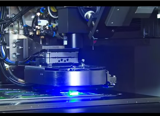
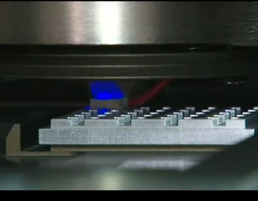
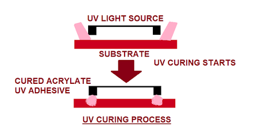
UV curing technology is very effective for controlling the pressure-sensitive adhesive properties of acrylic adhesive, because mechanical properties, surface tension, and miscibility are dramatically changed by UV irradiation. The thin wafers mounted on Die Attach Film (DAF) or die-bonding film for stacked die packages will be subjected to proper UV curing to avoid issues like dies flying off from the wafer during dicing, adhesive whiskering, and adhesive attachment or merging after dicing.
Therefore, UV cure is a crucial process step that the wafer should undergo to ensure the ideal adhesiveness of Die Attach Film (DAF) is achieved. Experimentation of the UV cure process parameters will be required to get the best performance for it based on production requirements. Typically, the process of UV curing is in the presence of a wavelength of 365nm to 400nm. Some Die Attach Film adhesives are easily curable in the presence of moisture, heat, and high light intensity. UV light usually requires a programmable intensity to the extent that a UV light profile is created.
5) Silver Sintering Die Attach:
Silver sintering is one of the most promising technologies for Die Attach. Due to their superior reliability properties as compared to conventional die Attach solder paste, dedicated reliability flow, and physical analyses can employ for sintering process optimization and durability assessment. The sintering layer degradation can be monitored during durability stress by scanning the acoustic microscopy and electric measurement of a temperature-sensitive electric parameter. The sintering layer is an option to substitute the solder joint from chips to carrier substrates. A reliable and stable bond can be manufactured considering a suitable combination of time, temperature, and pressure. Sintering joints have excellent thermal conductivity and have a very high melting point (about 962 °C for silver sintering) and they significantly reduce the amount of creep as compared to conventional solder compounds.

6) Thermocompression Die Bonding:
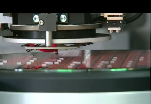
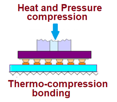
The thermocompression process is also known as diffusion bonding. It consists of heating and applying thermal and mechanical pressure to make atomic contact between two joining metals on-die bonding equipment. This atomic interaction sticks the interface together. The combined energy facilitates the diffusion of the metals, thus resulting in a metallurgical bond between the two surfaces.
7) Flip Chip Die Attach:
In Flip Chip Die Attach, the chip is flipped before being attached, and solder or conductive polymer bumps between chip and substrate serve as both an electrical and mechanical interconnection by Flip Chip Die Attach Equipment/Die Bonder. The basic flip-chip bonding process interconnection can be subdivided into three functional areas.
-
Under Bump Metallization (UBM)
The UBM is a compatible metal sandwich connecting the chip metallization (usually aluminum or copper) to the bump metallization and generally consists of an adhesion layer, a barrier layer, a wetting layer, and an anti-oxidation barrier.
-
IC bump and bond material
The IC bumps and Die Attach materials consist of a controlled amount of solder per interconnect, deposited by evaporation, electroplating, stencil printing, or solder jetting.
For this process, a higher melting temperature solder is needed for Flip Chip attachment. The Flip Chip die is mounted onto a laminate substrate together with other Surface Mount Device (SMD) components, a low melting temperature solder is usually preferred to form all interconnects on the board simultaneously.
