Nvidia jumps to FOPLP for AI server chips amid CoWoS capacity strain – DIGITIMES
Credit: DIGITIMES
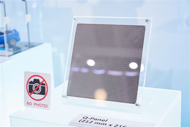
Nvidia is reportedly planning to adopt Fan-Out Panel Level Packaging (FOPLP) technology for its GB200 AI server chips ahead of schedule, aimed at addressing the tight production capacity of Chip on Wafer on Substrate (CoWoS) packaging at TSMC.
Industry insiders noted that FOPLP is poised to emerge as a prime alternative to CoWoS for packaging AI chips. This shift comes as chip vendors actively explore substitute solutions due to TSMC’s CoWoS capacity constraints and the surging demand for AI chips driven by the widespread adoption of generative AI applications.
A recent Chinese media report, citing a senior executive from China Wafer Level CSP, revealed that FOPLP technology offers potential advantages in cost reduction and capacity breakthrough, despite having weaker technical specifications compared to TSMC’s CoWoS due to its larger process size.
According to reports from AnandTech and SemiEngineering, FOPLP and FOWLP (Fan-Out Wafer Level Packaging) are now the two main types of fan-out packaging. FOPLP, emerging as a strong contender in fan-out packaging, is garnering industry attention for its lower costs and greater flexibility, although challenges remain.
An increasing number of packaging companies are gearing up to offer FOPLP services. However, a report from Yole Group suggests that FOWLP remains the mainstream carrier type in the overall fan-out packaging market, while FOPLP is still considered a niche market segment.
Despite its niche status, FOPLP’s market share is predicted to rise significantly, from 2% in 2022 to 8% by 2028, attributed to the expansion of panel-level packaging production lines and the cost-efficiency benefits of higher yields. As a result, FOPLP adoption is expected to outpace the overall fan-out packaging market, according to the report.
The report also highlighted that FOWLP and FOPLP have distinct development directions. FOWLP focuses on direct packaging on the wafer, resulting in smaller and highly integrated packages suitable for large chips like CPUs, GPUs, and FPGAs.
In contrast, FOPLP, through panel-level packaging, can fulfill a broader range of packaging needs, including high-power, high-current power semiconductors. In addition, FOPLP does not require the most advanced processes and equipment, making it a more accessible technology.
For semiconductor suppliers, the critical point in transitioning from FOWLP to FOPLP hinges on risks and costs. Thus, FOPLP must achieve significantly lower costs while delivering comparable outputs to FOWLP. Industry insiders highlighted that FOWLP’s established presence makes it difficult to convince customers to switch to FOPLP unless urgently needed.
FOPLP offers semiconductor suppliers a platform to create fully heterogeneous products by integrating chips from various wafer fabs or foundries, insiders continued. However, they stressed that widespread adoption will hinge on achieving cost parity and high yields with panel-level substrates.

