Nhóm do MIT dẫn đầu trình diễn đèn LED siêu nhỏ RGB xếp chồng theo chiều dọc, đầy đủ màu sắc
News: LEDs
6 February 2023
Much like transistors, LEDs are reaching a limit to how small they can be while also performing effectively. This is especially noticeable in close-range displays such as augmented-reality (AR) and virtual-reality (VR) devices, where limited pixel density results in a ‘screen door effect’ such that users perceive stripes in the space between pixels.
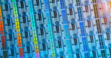
Now, a team led by Massachusetts Institute of Technology (MIT) has developed a new way to make sharper, defect-free displays (‘Vertical full-colour micro-LEDs via 2D materials-based layer transfer’, Nature volume 614, p81–87 (2023)). Instead of replacing red, green and blue light-emitting diodes side by side in a horizontal patchwork, the team has devised a way to stack the diodes to create vertical, multi-colored pixels.
Each stacked pixel can generate the full commercial range of colors and measures about 4μm wide. The micro-LEDs can be packed to a density of 5000 pixels per inch. “This is the smallest micro-LED pixel, and the highest pixel density reported in the journals,” says Jeehwan Kim, associate professor of mechanical engineering at MIT. “We show that vertical pixellation is the way to go for higher-resolution displays in a smaller footprint,” he adds.
“For virtual reality, right now there is a limit to how real they can look,” adds Jiho Shin, a postdoc in Kim’s research group. “With our vertical micro-LEDs, you could have a completely immersive experience and wouldn’t be able to distinguish virtual from reality.”
Kim and Shin’s co-authors include members of Kim’s lab, researchers around MIT, and collaborators from Georgia Tech Europe, Sejong University, and multiple universities in the USA, France and Korea.
Placing pixels
Most existing digital displays are lit through organic light-emitting diodes (OLEDs), but these can degrade over time, resulting in permanent burn-in effects on screens. The technology is also reaching a limit to the size the diodes can be shrunk, limiting their sharpness and resolution.
For next-generation display technology, researchers are exploring inorganic micro-LEDs, which could perform better, require less energy, and last longer than OLEDs.
But micro-LED fabrication requires extreme accuracy, as microscopic pixels of red, green and blue need to first be grown separately on wafers, then precisely placed on a plate, in exact alignment with each other in order to properly reflect and produce various colors and shades. Achieving such microscopic precision is a difficult task, and entire devices need to be scrapped if pixels are found to be out of place.
“This pick-and-place fabrication is very likely to misalign pixels in a very small scale,” Kim says. “If you have a misalignment, you have to throw that material away, otherwise it could ruin a display.”
Color stack
The MIT team has devised a potentially less wasteful way to fabricate micro-LEDs that doesn’t require precise, pixel-by-pixel alignment. The technique is a vertical LED approach, in contrast to the conventional, horizontal pixel arrangement.
Kim’s group specializes in developing techniques to fabricate pure, ultrathin, high-performance membranes, with a view toward engineering smaller, thinner, more flexible and functional electronics. The team previously developed a method for growing and peeling away perfect, two-dimensional, single-crystalline material from wafers of silicon and other surfaces — termed 2D material-based layer transfer (2DLT).
In the current study, the researchers employed this same 2DLT approach to grow membranes of red, green and blue LEDs of near-submicron thickness on two-dimensional material-coated substrates via remote or van der Waals epitaxy. Mechanical release then allowed each LED membrane to be peeled away from their base wafers, before they were stacked together to form layers of red, green and blue membranes. Top-down fabrication then patterned them into vertical pixels, each just 4µm wide.
“In conventional displays, each R, G and B pixel is arranged laterally, which limits how small you can create each pixel,” Shin notes. “Because we are stacking all three pixels vertically, in theory we could reduce the pixel area by a third.”
As a demonstration, the team fabricated a vertical LED pixel and showed that, by altering the voltage applied to each of the pixel’s red, green and blue membranes, they could produce various colors in a single pixel. “If you have a higher current to red, and weaker to blue, the pixel would appear pink, and so on,” Shin says. “We’re able to create all the mixed colors, and our display can cover close to the commercial color space that’s available.”
The team plans to improve the operation of the vertical pixels. So far, they have shown that they can stimulate an individual structure to produce the full spectrum of colors. They will work toward making an array of many vertical micro-LED pixels.
“You need a system to control 25 million LEDs separately,” Shin says. “Here, we’ve only partially demonstrated that. The active matrix operation is something we’ll need to further develop.”
“For now, we have shown to the community that we can grow, peel and stack ultrathin LEDs,” Kim says. “This is the ultimate solution for small displays like smart watches and virtual-reality devices, where you would want highly densified pixels to make lively, vivid images.”
The research was supported, in part, by the US National Science Foundation (NSF), the US Defense Advanced Research Projects Agency (DARPA), the US Air Force Research Laboratory (AFRL), the US Department of Energy, LG Electronics, Rohm Semiconductor, the French National Research Agency, and the National Research Foundation in Korea.

