[News] Intensified Competition in the Semiconductor Industry for 2nm Technology Dominance, Potentially Reshaping the Global Foundry Market – TrendForce
The competition for dominance in 2nm semiconductor technology has intensified at the beginning of 2024, marking a crucial battleground among global foundry companies.
As per a report from IJIWEI, major foundry enterprises such as Samsung Electronics, TSMC, and Intel are set to commence mass production adopting 2nm process starting this year. Consequently, the fierce competition for supremacy in 2nm technology is expected to escalate from 2025 onwards. Currently, the most advanced production technology globally is at the 3nm level.
TSMC’s 2nm products will be manufactured at the Fab 20 in the Hsinchu Science Park in northern Taiwan and at a plant in Kaohsiung.
The Fab 20 facility is expected to begin receiving related equipment for 2nm production as early as April, with plans to transition to GAA (Gate-All-Around) technology from FinFET for 2nm mass production by 2025.
During TSMC’s earnings call on January 18th, TSMC revealed that its capital expenditure for this year is expected to fall between USD 28 billion and 32 billion, with the majority (70% to 80%) allocated to advanced processes. This figure is similar to that of 2023 (USD 30.4 billion), indicating stable investment to ensure its leading position in 2nm technology.
After announcing its re-entry into the foundry business, Intel is actively advancing its foundry construction efforts. The plan includes the introduction of the Intel 20A (equivalent to 2nm) process in the first half of 2024 and the Intel 18A (1.8nm) process in the second half of the year. It is understood that the Intel 18A process will commence test production as early as the first quarter of this year.
Intel’s 2nm roadmap is more ambitious than originally anticipated, being accelerated by over six months. In response to criticisms of its “overly ambitious” plans, Intel swiftly began procuring advanced Extreme Ultraviolet (EUV) equipment.
Samsung Electronics has devised a strategy to gain an advantage in the more advanced process war through its Gate-All-Around (GAA) technology. Currently, it is mass-producing the first-generation 3nm process based on GAA (SF3E) and plans to commence mass production of the second-generation 3nm process this year, significantly enhancing performance and power efficiency.
Regarding the 2nm process, per a report from Nikkei, Samsung plans to start mass production for mobile devices in 2025 (SF2) and gradually expand to high-performance computing (HPC) in 2026 and automotive processes in 2027.
Currently, Samsung Electronics is producing GAA products for the 3nm process at its Hwaseong plant and plans to manufacture products for both the 3nm and 2nm processes at its Pyeongtaek facility in the future.
Rapidus, a chip manufacturing company supported by the Japanese government, is expected to trial-adopt 2nm process at its new plant by 2025 and begin mass production from 2027.
If Rapidus’ technology is validated, the global foundry market may expand beyond the Taiwan-Korea duopoly to include Taiwan, Korea, the United States, and Japan.
The technology competition to become a “game-changer” ultimately depends on the competition for customers. It’s rumored that TSMC holds a leading position in the 2nm field, with Apple speculated to be its first customer for the 2nm process. Graphics processing giant NVIDIA is also considered a major customer within TSMC’s client base.
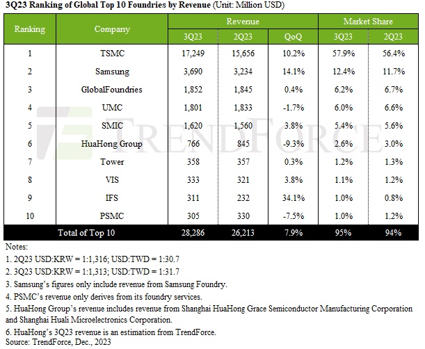
According to TrendForce data as of the third quarter of 2023, TSMC’s revenue share accounted for a dominant 57.9%, with Samsung Electronics trailing at 12.4%, a gap of 45.5 percentage points.
However, Samsung Electronics is not sitting idly by. With continuous technological investment, Samsung’s foundry customer base grew to over 100 in 2022, a 2.4-fold increase from 2017. The company aims to expand this number to around 200 by 2028.
Particularly, Samsung’s early adoption of GAA technology is expected to give it an advantage in achieving early production volumes for advanced processes.
Read more
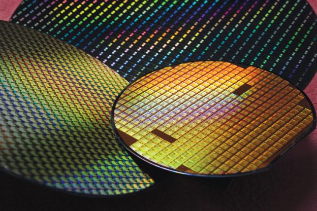
(Photo credit: TSMC)

