National Semiconductor Technology Center Taking Shape – AIP.ORG
Share
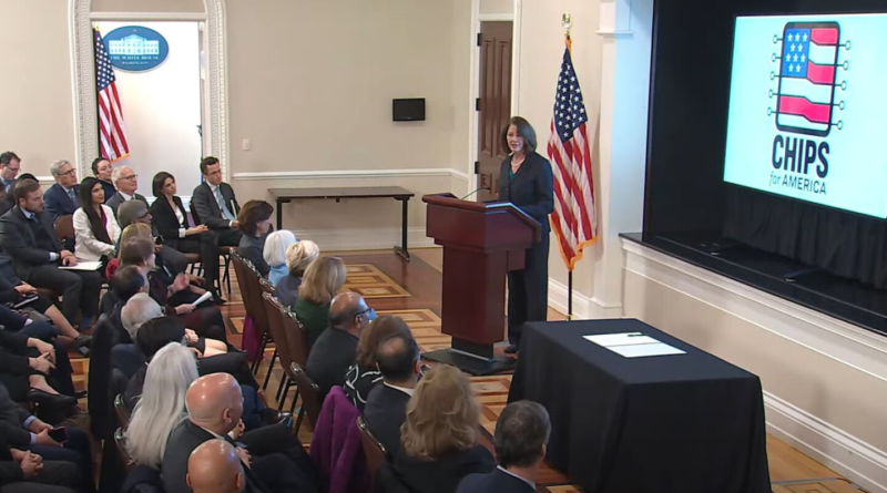
Deirdre Hanford, head of the operating entity for the National Semiconductor Technology Center, speaks at a White House event held to mark an interagency agreement on NSTC oversight.
(The White House)
The White House announced today that it plans to allocate more than $5 billion for semiconductor R&D and workforce training through the National Semiconductor Technology Center (NSTC), a public-private entity that is being created to administer the funds. The money will come out of the $11 billion in semiconductor R&D funds appropriated to the Commerce Department by the CHIPS and Science Act of 2022.
The NSTC will be operated by a non-profit entity called the National Center for the Advancement of Semiconductor Technology, or Natcast, which launched in November 2023. Early this year, Natcast appointed as its CEO Deirdre Hanford, a longtime executive at Synopsys, which produces tools that aid in chip design.
Natcast intends to launch its first research funding opportunity sometime in the first half of 2024, though it has not yet announced where the NSTC will be physically located. The NSTC will consist of a headquarters and a geographically distributed network of “affiliated technical centers,” according to a vision paper the department released in April 2023.
The White House held an event today to mark the signing of an interagency agreement on next steps for establishing the NSTC Consortium, which will oversee Natcast. The agreement is not public, but the Commerce Department anticipates making it public at some point, according to a department spokesperson.
A summary on the NSTC website explains that the agreement “outlines the goals and processes for determining the strategy and membership structure of the NSTC Consortium.”
“The NSTC Consortium is not a legal entity and does not have a staff. Rather, it has a steering committee as its governing body, and will include members from a wide range of stakeholders including industry, academic institutions, investors, and government bodies. As a new purpose-built, non-profit entity, Natcast was created to operate the programs of the NSTC Consortium,” the website explains.
Hanford spoke at the White House today on Natcast’s next steps. “You’re looking at employee number one of one. So, if you’re interested in a job, please come find me,” Hanford said. Natcast is also seeking community input on what its priorities should be through a new survey for prospective participants, Hanford added.
Commerce Secretary Gina Raimondo said at the event that an early priority for NSTC will be to establish a “workforce center of excellence.” She described the center as “the national hub for all workforce development efforts in the semiconductor industry — everything from high schools to community colleges to the most sophisticated PhDs in America.”
The White House stated in a press release that the goal is to launch NSTC’s “workforce activities” this summer, which will include participation from the National Science Foundation and other agencies. NSF received $200 million from the CHIPS and Science Act specifically for semiconductor workforce development.
Other participants in the event included White House Office of Science and Technology Policy Director Arati Prabhakar, NSF Director Sethuraman Panchanathan, Deputy Defense Secretary Kathleen Hicks, Energy Secretary Jennifer Granholm, and National Institute of Standards and Technology Director Laurie Locascio.
Locascio highlighted recent funding announcements by other R&D programs funded through the $11 billion appropriated by the CHIPS and Science Act.
NIST announced on Feb. 1 that it will spend at least $200 million over five years to establish a Manufacturing USA Institute focused on creating “digital twin” computer models of key semiconductor manufacturing and packaging technologies. The agency also announced the same day that the first funding opportunity issued by the planned National Advanced Packaging Manufacturing Program (NAPMP) will provide about $300 million over five years for R&D on materials and substrates used in semiconductor packaging.
Locascio said this funding opportunity represents the first of six focus areas for the packaging program, which will have a total budget of about $3 billion. She also explained that the intent is to create a “facilities ecosystem” that will include the digital twins institute, an advanced packaging prototype facility, and a “flagship prototyping facility” run by the NSTC.
In parallel with these R&D initiatives, the Commerce Department is gearing up to begin distributing awards from the $39 billion appropriated by the CHIPS and Science Act to subsidize domestic semiconductor manufacturing. So far the department has announced two preliminary awards that are relatively small, but larger awards are imminent.
“In the coming 6 to 12 weeks you’re going to see a drumbeat of even bigger announcements,” Raimondo said.
American Institute of Physics advances, promotes and serves the physical sciences for the benefit of humanity.
AIP is a 501(c)(3) not-for-profit corporation. Together with our Member Societies, we convey a unifying message for stakeholders in government, academia, the nonprofit and private sectors.
American Institute of Physics advances, promotes and serves the physical sciences for the benefit of humanity.
AIP is a 501(c)(3) not-for-profit corporation. Together with our Member Societies, we convey a unifying message for stakeholders in government, academia, the nonprofit and private sectors.
© 2024. American Institute of Physics
