Mô hình hóa GaN HEMT với các tham số ANN hướng đến khả năng mở rộng
Designers choosing gallium nitride (GaN) transistors may face a surprising challenge when putting the devices in their context. While the Advanced SPICE Model for GaN HEMTs (ASM-HEMT) model captures many behaviors like thermal and trapping effects, it grapples with accuracy over a wide range of bias conditions. Foundries often define ASM-HEMT parameters from measurements at a specific bias point but don’t solve for different bias values. Keysight device modeling researchers are exploring an improved ASM-HEMT hybrid model, blending measurements with physics and using artificial neural network (ANN) techniques for improving wide-range S-parameter fit in minutes. We spoke with Rafael Perez Martinez, R&D Software Engineer in the R&D Device Modeling group at Keysight EDA, about this new approach to GaN HEMT modeling with ANN parameters.
A choice between lengthy measurements or less-than-accurate simulations
Perez Martinez began his exploration of GaN HEMT modeling at Stanford University, working on his PhD in the Wide-Bandgap Lab (WBGL). “I had an idea in 2022 looking at prior ASM-HEMT publications. It seemed like people weren’t reporting CV characteristics fitting, and they tended to fit the model at one drain voltage bias,” he says. “Measurements are tedious, and measurement-based models such as DynaFET require extensive DC and S-parameter data and large-signal non-linear vector network analyzer (NVNA) measurements that can take one to three months to set up and execute.” Physics-based theoretical models like ASM-HEMT can readily simulate and extend S-parameter predictions across frequency ranges but tend to inaccurately fit parameters at varying bias voltages.
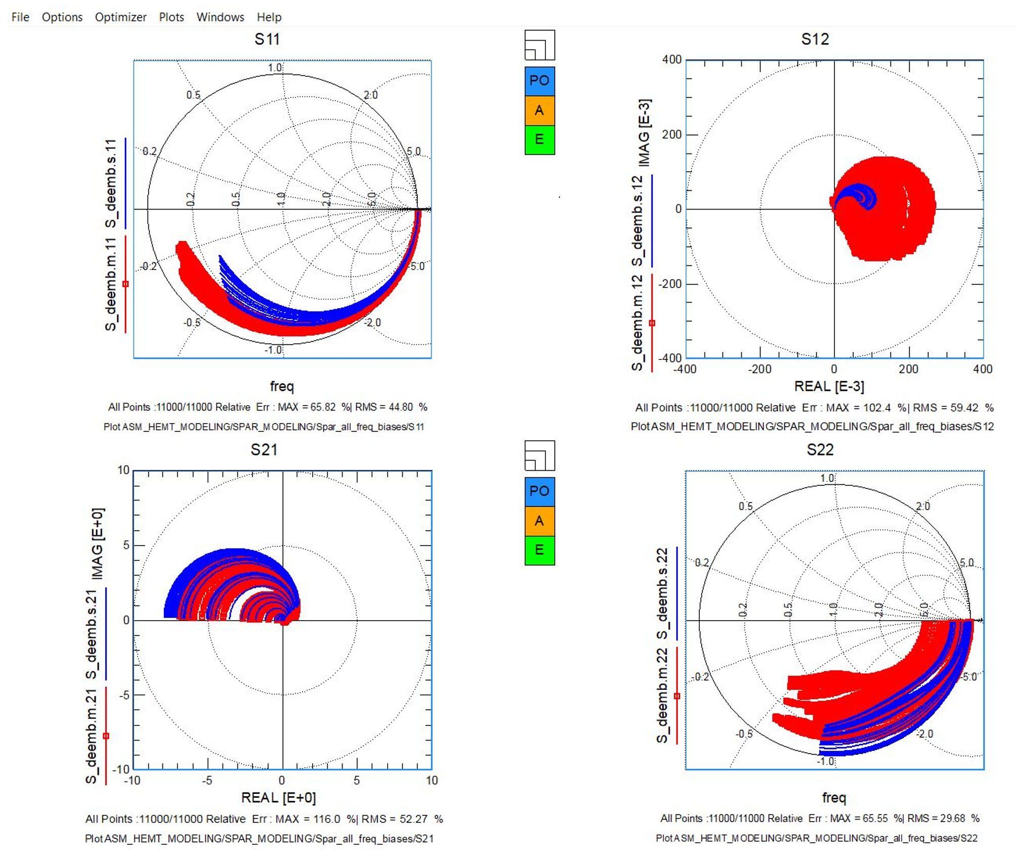
Additionally, many university labs and start-ups don’t have budgets for an NVNA or similar instruments and accessories for GaN HEMT measurements. Perez Martinez parlayed his summer internships at Keysight into a WBGL proposal for grant funding for a Keysight PNA-X, which arrived at the lab in 2023. With coaching from Keysight teams, Perez Martinez dove in, taking PNA-X readings on a 150nm gate length GaN-on-SiC HEMT and capturing its non-linear characteristics. Plugging the measured parameters as-is into a standard ASM-HEMT model highlighted the disparity between the two approaches. The S-parameter fitting performs poorly with VD=5 to 25 V, VG=-3 to -1V, and f = 250MHz to 50GHz (measurements in red, simulations in blue).

Moving to hybrid GaN HEMT modeling with ANN parameters
This persistent mismatch between measurements and simulation gave Perez Martinez the idea of developing a hybrid model example, combining the baseline of a measurement-based model with the extensibility and speed of physics-based modeling. “I had GaN HEMT measurements at 10 GHz with second and third harmonics,” he says. “But starting the hybrid model was difficult initially because you need to know the device model, go through the Verilog code, know what to change – and you can’t just add things randomly. There has to be some physical aspect of any change that makes sense.”
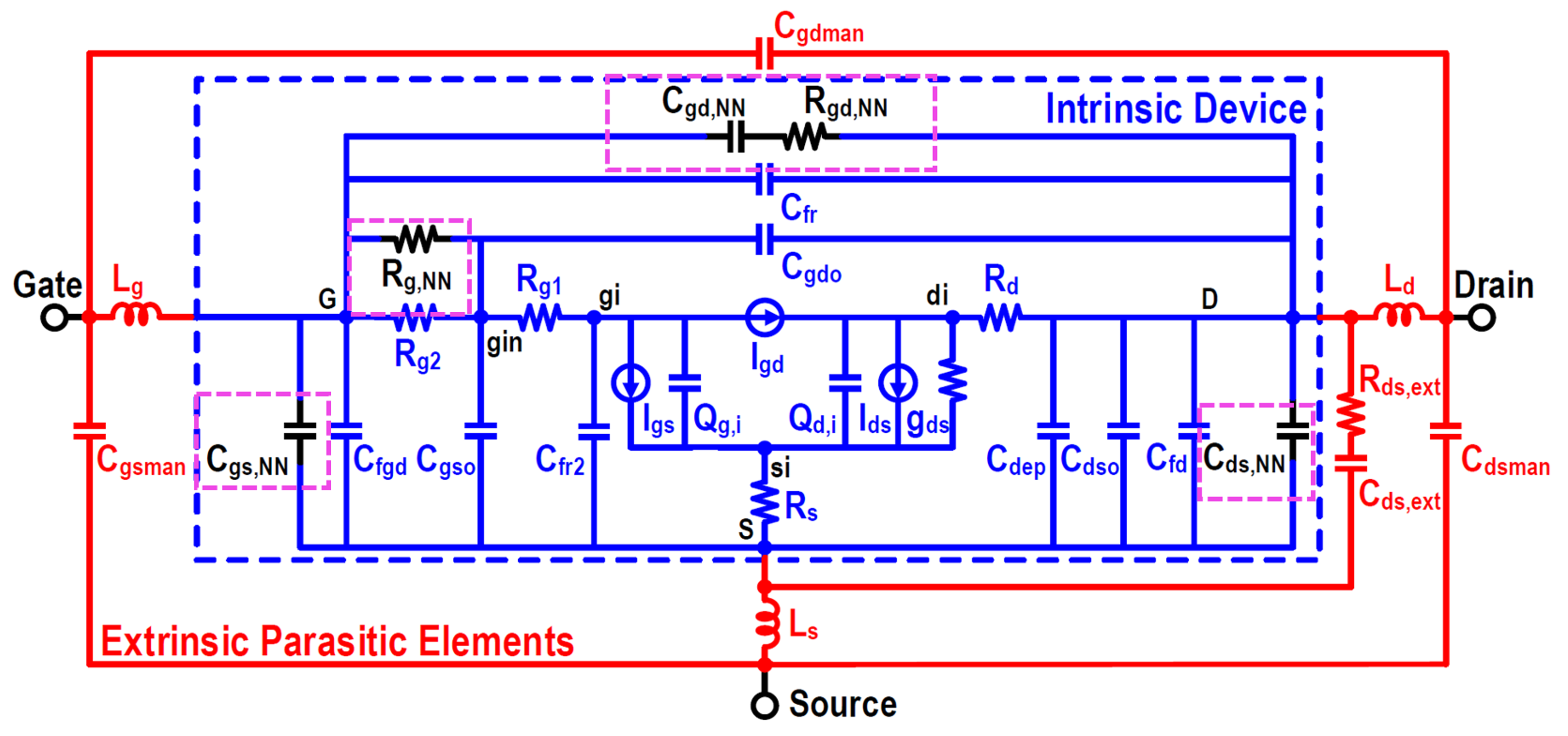
With measurements in the 10 GHz region where the model should be most accurate, Perez Martinez moved into Keysight IC-CAP for modeling with its ANN Modeling Toolkit. “Integrating a neural network into the Verilog model is quite trivial using the ANN toolkit,” continues Perez Martinez. “Looking at some earlier small-signal models, I noticed the ASM-HEMT model was missing something around gate-drain resistance, so that’s where I started, working carefully not to fix one problem and break something else.” A few cycles of replacing parameters with ANN variables and using the IC-CAP optimizer added two resistances and three capacitances to the ASM-HEMT equivalent circuit (inside the dotted pink outlines).

Generalizing results from ANN parameter fitting
A Keysight ADS simulation with hybrid ANN parameters from IC-CAP aligns very closely with measurements, as indicated by the near-perfect overlap between the red lines and the dotted pink lines in this comparison of power-added efficiency, gain versus Pout, and dynamic load lines. In this case, the model modification solves the problem of simulating wide-range bias.

The logical follow-up to this result: are these results device-specific, or will the methodology scale to smaller geometries and higher frequencies? “The first challenge is getting measurements at higher frequencies, which takes access to instrumentation, plus time and care,” observes Perez Martinez. “The next challenge is not every GaN HEMT has the same physical device structure, and people tend to play tricks – maybe the distance between the drain and gate varies, maybe there’s a different field plate, or maybe the gate structure has a different shape.” The implication is that one model may not fit all devices. However, the ANN approach in IC-CAP works with any device model and helps narrow down where modifications can improve and speed up S-parameter fitting – in a matter of hours versus months of measurements.
That’s an important observation since Perez Martinez is not necessarily looking for a formal ASM-HEMT model update. He’s presenting his paper at the IEEE BiCMOS and Compound Semiconductor Integrated Circuits and Technology Symposium (BCICTS) to raise awareness and generate discussion around the approach. “People always talk about positive results in papers, but rarely do they talk about the failures it took to get there,” says Perez Martinez. “This is really a look at some GaN HEMT model shortcomings we’ve seen, and a hybrid model example in IC-CAP with ANN that we’d like people to look at that might fit their needs.”
To see more details about the methodology for GaN HEMT modeling with ANN parameters and the results, see the BCICTS 2024 paper in the BCICTS proceedings archive:
A Hybrid Physical ASM-HEMT Model Using a Neural Network-Based Methodology
Also, see more information on the latest in GaN device modeling from Keysight experts:
Electronic Design webinar: Mastering GaN Device Modeling
Keysight: Device Modeling IC-CAP | W7009E PathWave IC-CAP ANN Modeling Toolkit
Share this post via:

