ML và Multiphysics Corral 3D và HBM
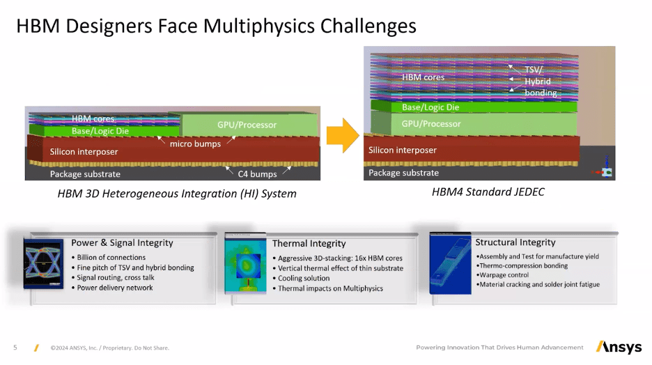
3D design with high-bandwidth memory stacks (HBM) has become essential for leading edge semiconductor systems in multiple applications. Hyperscalers depend on large AI accelerator cores supported by 100GB or more of in-package HBM to handle trillion parameter AI models. Autonomous Drive (AD) vehicles may handle smaller individual tasks but more of them through multiple levels of sensing and fusion support, computer vision, graphics, safety, security, and communication objectives. Similar requirements are appearing in aerospace and other applications. All require 3D integration with HBM to maximize performance, minimize latency, and minimize power consumption. Manufacturing technologies to build such systems are already in place but optimizing such a design introduces new physics challenges in performance and reliability.

The Physics of Large System Design
There’s only so much circuitry you can fit on a single silicon die, even in the most advanced processes. Bigger designs must split across multiple chiplets (die) but can now connect very effectively inside a single package, greatly reducing the performance and power hit compared to an equivalent circuit between packaged components on a PCB. The advantage is especially clear for large memory access implemented as stacked HBM chiplets within the same package, for which access latencies are greatly improved over off-chip DRAM.
Managing the physics of large semiconductor designs was already prominent before multi-chiplet designs appeared. Beyond the usual design objectives (functionality, performance, power and area/cost) a product design team must optimize for: over-heating with potential to damage/compromise the system; inadequate power distribution for functional demand undermining performance and reliability; electronic crosstalk impacting signal integrity; die/chiplet warping through heating resulting in broken bond connections. Tools to analyze these factors for a single die are already familiar and a well-understood strength for Ansys: power integrity (EM/IR) analysis, thermal analysis, signal integrity and mechanical analysis coupled with thermal.
Scaling multiphysics analysis up to multi-chiplet designs introduces new challenges. Thermal becomes a bigger issue especially in stacked structures where thin chiplet substrates provide little thermal isolation between layers. This analysis problem isn’t just bigger than for an already complex single die multiphysics analysis; in a 3D/HBM structure all these factors are coupled and must be co-optimized.
Multiphysics, Coupling and ML
Lang Lin (Principal Product Manager at Ansys) gave an excellent webinar talk recently on this topic, illustrating with emphasis on an HBM stack, sitting on top of a logic die and next to CPUs or GPUs on the interposer. One point he made is that traditional PVT (process-voltage-temperature) corner analysis for a single die won’t necessarily work for analysis of a complete structure of stacked chiplets. In an HBM stack, chiplets may have different assembly corners due to coupling effects. One might best be assigned a temperature of 90 degrees, at 0.8 volts and a fast-fast process. Another (in the same stack) should be assigned a temperature of 100 degrees, 0.9 volts and a typical-typical process. And so on, down the stack. Raising an obvious question – how do you figure this out?
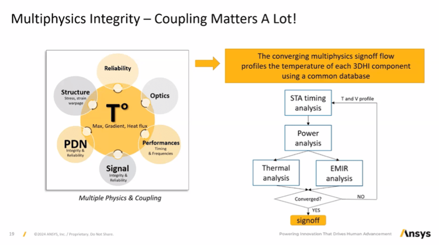
A key point Lang made is that physics factors in this tightly packed environment are strongly coupled and all centered around thermal considerations.

Coupling implies that you can’t just optimize for one factor at a time. Temperature affects the power delivery network, timing, signal integrity which in turn can affect temperature. In a heterogenous integration with HBM, CPUs, GPUs, etc., etc., optimizing across all these factors would become a nightmare. Converging to an optimal physics solution requires (no surprise) intelligent and automated guidance. Ansys accomplishes this through their OptiSLang system which will search intelligently through vast parametric spaces to find robust solutions automatically. I’m convinced this is the way of the future in system level optimization tasks of all kinds.
Ground Proofs
Lang illustrated with a couple of live examples, the first working with TSMC on HBM optimization for warpage/stress in assembling a stack, which can result in yield loss. Here thermal cycling is based on manufacturing requirements rather than on use-cases, however I would think that temperature ranges they show in manufacturing are at least as stressful as in mission mode. TSMC and Ansys used the flow to estimate warpage/stress at each assembly step, to come up with an optimal manufacturing assembly sequence.
In another case study, Ansys worked with a different company to optimize the signal integrity of high-speed HBM interconnect (connecting to compute chiplets) on a 2.5D interposer. Here they were able to propose an optimal routing pattern for the multi-bit interconnect to minimize (transmission line) overshoot.
Pretty impressive. You can register to watch the webinar HERE.
Also Read:
A Master Class with Ansys and Synopsys, The Latest Advances in Multi-Die Design
Synopsys-Ansys 2.5D/3D Multi-Die Design Update: Learning from the Early Adopters
Share this post via:
