Loại bỏ đường dẫn sai chức năng trong quá trình phân tích RDC
Reset domain crossing (RDC) issues can occur in sequential designs when the reset of a source register differs from the reset of a destination register, even if the data path is in the same clock domain. This can lead to asynchronous crossing paths and metastability at the destination register. RDC analysis on RTL designs is done to find such metastability issues in a design, which may occur during the assertion of asynchronous resets between two adjacent registers. More reset domains and asynchronous resets in modern chips, along with faster designs, requires a proper reset domain crossing sign-off methodology to avoid chip-killing metastability problems and other functional problems.
The growth in reset domains is driven by complex SoCs utilizing different controllers to manage more complex power management schemes. Also contributing to this increase are security management schemes, I/O components, and functional configurations from different sources that can run at different clock frequencies, as well as power-up resets and software-based resets.
A decade ago, static verification technologies were a “nice to have.” Today, in an environment of ever-increasing design complexity, static verification is now so non-trivial that design and verification teams along with EDA vendors continue investigating newer checks and methodologies for static analysis. The cost and schedule impact of design issues caught late in the design cycle have made engineers focus on RDC analysis of RTL designs. Fixing RDC bugs properly often requires changing the reset architecture, which can be very costly at a late stage in the design cycle. Additionally, a poorly architected reset strategy can lead to reset bugs escaping to silicon, thereby leading to the prejudicial wasting of thousands or even millions of dollars, design respins, and slipping project schedules.
What is reset domain crossing
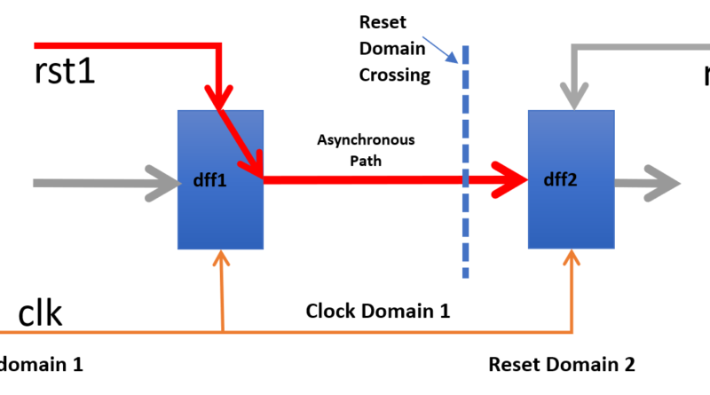
A reset domain crossing occurs when a path’s transmitting register has an asynchronous reset, and the receiving register has an uncorrelated reset or no reset. Design errors that can occur from improperly implemented reset domain crossings and asynchronous resets are metastability and loss of functional correlation.
Fig. 1: Reset domain crossing path.
Due to their increasing prevalence in SoC designs, design teams are “shifting-left” RDC analysis and sign-off as part of their strategy to gain confidence that their designs are functionally correct before going to silicon.
Avoid using constraints to filter out functional false Paths in RDC
Engineers tend to take an easy route to completely eliminate paths from analysis by setting false path constraints, but this is no better than a waiver and can result in bugs. It is our belief that any RDC tool should automatically recognize functional false paths and report them. Functional false path reporting by the tool has many advantages. The first and foremost is that all the domain crossing paths are analyzed by the tool. Some EDA tools apply formal verification technology to report these types of paths (even if unconstrained by the user). Doing so provides confidence that all the paths are analyzed. Additionally, engineers can make necessary changes to the design at an early stage of design development to address domain crossing issues identified by the tools. The proposal we support involves analyzing these paths under a different RDC scheme.
Automatic recognition of functional false paths in RDC
Engineers writing RTL often don’t realize that some paths, which may cause RDC paths between a transmit source and a receive destination, are functionally false. These paths may not cause any functional failure in the design, and these false paths can be ignored in functional verification. Synthesis tools also don’t have a way to identify these functionally false paths, but during RDC analysis, these paths will appear as RDC violations if an RDC exists between the transmit source and receive destination. These RDC violations are considered noise in RDC analysis results. Depending on how many such paths exist in a design, reviewing and addressing these issues can be an inefficient, time-consuming effort, that wastes valuable time.
Now let’s look at how an RDC tool is able to identify these paths automatically as functionally false paths and identify them as safe paths. This reduces the amount of time and effort an engineer must spend analyzing and debugging RDC results.
Case 1 – Consider the schematic in figure 2. There is an RDC crossing between the transmit source “t1” and the receive destination “out.” These two registers are driven by the same clock but have different asynchronous resets. Looking at the path between the two registers, there are multiple muxes on the path. When the select pin is set to “0” for the first mux, the “D0” pin is selected, which is connected to the output pin of the transmit source register “t1.” For the second mux, the “D0” pin is not connected to the “t1” register, but it is connected to a different transmit source “in2.” When the select pin is set to “1” for the first mux, “D1” is selected, which is set to a constant “0.” Hence, the path between “t1” and “out” can be considered as a functionally false path, and no RDC violation should be reported. If a design has hundreds or even thousands of these functionally false paths, engineers won’t spend their time unnecessarily debugging them. Solutions without this capability will report these paths as domain crossing errors that will require time and effort to debug.
Fig. 2: Functional false path for RDC.
Case 2 – Consider the schematic in figure 3. There are two possible RDC crossings between the transmit source “d1,” the receive destination “s0” and the transmit source “d2” and receive destination “s0.” All the registers are driven by the same clock. But the “d1” and “d2” registers are driven by the asynchronous reset “rstn1,” and the “s0” register is driven by a different asynchronous reset, “rstn2.” If we write the Boolean expression for the combinatorial logic between the transmit source and receive destination registers, it is ((!din1 & din2) + (din1 & din2)). This expression can be written as ((!din1 + din1) & din2). Which can further be simplified as “din2” only. So, the RDC path between “d2” and “s0” is a valid RDC path that needs to be evaluated. The RDC analysis tool classifies the path between “d1” and “s0” as a functionally false path.
Fig. 3: Functional false path for RDC.
Conclusion
In this article, we highlighted specific issues that must be addressed by designers to improve RDC results and to ensure the highest fidelity in identifying real design issues. Due to noisy results during RDC analysis, engineers may get overwhelmed by the large the number of violations. This may cause delays in closing RDC analysis, which may impact the overall project schedule.
Evaluating the results from RDC analysis can take a significant amount of time to both understand and recognize the specific fault highlighted in the identified paths. The benefit of the analysis tool reducing the number of paths to review, through FFP detection and stable path inference, reduces the time spent by the reviewer, while allowing a more directed focus on the identified, real issues that should be addressed in the design.
To learn more about how analysis tools can save your team time and money while improving the quality of RDC results in your designs, please read the new white paper from Siemens EDA, Analysis of RDC Issues for Identifying Reset Tree Design Bugs for Noise Reduction.
Farhad Ahmed
Farhad Ahmed is a principal product engineer in the IC Verification Solutions division of Siemens EDA Software. He has been working in chip design and EDA companies for over 30 years, starting out as an RTL logic designer for Sun Microsystems working on SPARC microprocessors. Ahmed is currently the Secretary of the Accellera Clock Domain Working Group. He graduated with a B.Sc.(EE) degree from Bangladesh University of Engineering and Technology and a M.Sc.(EE) from Washington State University.


