Leveling up scanning electron microscope measurements for chip manufacturing – Phys.org
Click here to sign in with or
Forget Password?
Learn more
share this!
2
2
Share
Email
May 31, 2023
This article has been reviewed according to Science X’s editorial process and policies. Editors have highlighted the following attributes while ensuring the content’s credibility:
fact-checked
trusted source
proofread
by National Institute of Standards and Technology
Researchers from the National Institute of Standards and Technology (NIST) and KLA Corporation, a provider of inspection and measurement systems for the semiconductor and related industries, have improved the accuracy of scanning electron microscope (SEM) measurements. Used for process control applications in semiconductor manufacturing, SEMs help ensure high-yield production of functional, high-performance chips.
A SEM uses a focused electron beam to image features as small as one nanometer, making it an important instrument for characterizing semiconductor device structures. During chip manufacturing, high-resolution SEMs are used for many inspection and metrology applications, including detection of very small defects, identification and classification of defects found by optical inspectors, critical dimension measurements of pattern features, overlay measurements, and more. This information helps chip engineers characterize and fine tune their manufacturing processes.
As the electron beam travels through a SEM, it is carefully controlled. A slight deviation of the electron beam from the ideal path or a tiny misalignment of the angle at which the beam strikes the surface of the chip can distort the resulting SEM image and misrepresent the structure of the device. NIST and KLA improved the accuracy of SEMs by accounting for these angular misalignments of the electron beam. The joint research project measures beam tilt with an accuracy of less than one milliradian, or five hundredths of a degree, which required advances in angular resolution and measurement validation.
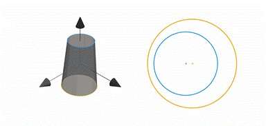
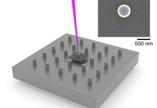
To measure the beam tilt, NIST and KLA created a prototype standard for electron microscopy and analyzed the resulting electron micrographs in a new way. The prototype standard consists of an array of tapering pillars of silicon, known as conical frusta, which form images that are highly sensitive to beam tilt. The tilt shows up as a shift between the centers of images of the top and bottom edges of a frustum. Using their expertise in modeling electron–matter interactions, the researchers used simulations to demonstrate the potential for sub-milliradian accuracy, guiding their ongoing design and fabrication of the standard artifacts.

Arrays of conical frusta at known positions have the potential to measure any variation of the beam tilt across the region scanned and imaged by the SEM. Those measurements could further calibrate the magnification and distortion of the electron microscope. Furthermore, the new standard has applications to other microscopy methods used in chip manufacturing, including atomic-force and super-resolution optical microscopy. The ability to compare the results of different microscopy methods helps to reliably and reproducibly transfer information between the different methods and improve the accuracy of measurement models.
“Electron-beam tilt shifts the apparent positions of device features, reducing the accuracy of SEM measurements,” said Andrew C. Madison, NIST researcher and first author on industry papers covering this research. “Our new standard and analysis method can detect electron-beam shift as it varies across the imaging field.”
“With this data, SEM manufacturers can implement calibrations and corrections that improve image quality and measurement accuracy,” said NIST researcher and principal investigator Samuel M. Stavis.
“As experts in semiconductor inspection and metrology, we’re continually exploring new technologies that can extend current measurement limits,” said Yalin Xiong, senior vice president and general manager at KLA Corporation. “Collaboration with research organizations serves an important role in discovering innovations that can help advance process control for the chip industry. Our joint research with NIST is aimed at improving the accuracy of the fundamental measurements used to characterize chip manufacturing processes.”
NIST plans to make the new standard and analytical method broadly available to the chip manufacturing industry and the scientific community through publications and eventual distribution of frustum arrays.
More information: A.C. Madison et al, Proc. SPIE 12496, Metrology, Inspection, and Process Control XXXVII, 1249606 (2023); doi.org/10.1117/12.2673963
Provided by National Institute of Standards and Technology
More information: A.C. Madison et al, Proc. SPIE 12496, Metrology, Inspection, and Process Control XXXVII, 1249606 (2023); doi.org/10.1117/12.2673963
Provided by National Institute of Standards and Technology
Explore further
Facebook
Twitter
Email
Feedback to editors
15 hours ago
1
17 hours ago
1
18 hours ago
0
May 25, 2024
1
May 24, 2024
1
4 hours ago
13 hours ago
13 hours ago
14 hours ago
14 hours ago
15 hours ago
15 hours ago
15 hours ago
17 hours ago
17 hours ago
May 26, 2024
May 22, 2024
May 17, 2024
May 14, 2024
May 12, 2024
May 10, 2024
More from Optics
Feb 20, 2023
Dec 22, 2021
Apr 11, 2022
Mar 3, 2023
Mar 31, 2022
Dec 14, 2017
18 hours ago
May 23, 2024
May 23, 2024
May 23, 2024
May 22, 2024
May 22, 2024
Use this form if you have come across a typo, inaccuracy or would like to send an edit request for the content on this page. For general inquiries, please use our contact form. For general feedback, use the public comments section below (please adhere to guidelines).
Please select the most appropriate category to facilitate processing of your request
Thank you for taking time to provide your feedback to the editors.
Your feedback is important to us. However, we do not guarantee individual replies due to the high volume of messages.
Your email address is used only to let the recipient know who sent the email. Neither your address nor the recipient’s address will be used for any other purpose. The information you enter will appear in your e-mail message and is not retained by Phys.org in any form.
Get weekly and/or daily updates delivered to your inbox. You can unsubscribe at any time and we’ll never share your details to third parties.
More information Privacy policy
We keep our content available to everyone. Consider supporting Science X’s mission by getting a premium account.
Medical research advances and health news
The latest engineering, electronics and technology advances
The most comprehensive sci-tech news coverage on the web

