Làm Chủ Đồng TSV Điền Phần 2/3

Establishing void-free fill of high aspect ratio TSVs, capped by a thin and uniform bulk layer optimized for removal by CMP, means fully optimizing each of a series of critical phases. As we will see in this 3-part series, the conditions governing outcomes for each phase vary greatly, and the complexity of interacting factors means that starting from scratch poses an empirical pursuit that is expensive and of long duration.
Robust and void-free filling of TSVs with copper progresses through six phases as laid out below:
- Feature wetting and wafer entry (previous article)
- Feature polarization
- Nucleation
- Fill propagation
- Accelerator ejection
- Bulk layer plating
- (Rinsing and drying, which we won’t cover in this series)
Feature Polarization
Before we talk about features specifically, let’s briefly review electrolyte formulation. In general, copper TSV plating chemistries are formulated of certain inorganic components and certain organic components. The inorganics are: deionized water, copper sulfate, sulfuric acid and hydrochloric acid. And the organics are commonly referred to as accelerator, suppressor and leveler. We could get very deep into the specifics here, and they are truly fascinating. However, we are not attempting to invent a TSV chemistry, but rather to put an existing one to use.
We ended the previous article having described wafer entry. In most cases, this entry step is followed directly by a brief “dwell step” during which the wafer simply sits in the electrolyte, ideally spinning at moderate speed, with no potential applied (thus no current flowing). During this step, the chemical affinity of the suppressor for the copper will cause the suppressor (and leveler as well) to adsorb to the surface. Complete coverage of the surface is critical as any location that is under-suppressed will experience unwanted copper growth. A previous colleague of mine used to refer to the effectiveness of this suppressor coverage as forming either a “blanket” of suppressor or an “afghan” of suppressor.
After the brief dwell step, the recipe moves into its first plating step. Here is where proper polarization plays out (or doesn’t!) Suppressors and accelerators operate in a sort of competition with each other in copper fill. Thus the specific formulations and relative concentrations matter very much in terms of the effectiveness of a given plating chemistry. Suppressors have an advantage over accelerators in that they absorb more readily. But accelerators have an advantage in that they diffuse more rapidly.
Given this, we can quickly understand how polarization plays out. All the components of the chemistry have equal access to the surface of the wafer as soon as it enters the bath. But suppressors dominate adsorption on the surface because they adsorb more readily, even in the presence of ample accelerator. However, all components need to travel down the via hole in order to adsorb in there. And this is where the advantage goes to the accelerator. Yes, it is a slower adsorber (spell check says that’s not a word), but because it gets to the bottom of the via before the other additives, it has the time it needs. A distribution thus forms wherein suppressor adsorption manifests at a very high concentration at the top of the via and accelerator adsorption manifests at a very high concentration at the bottom.
The blanket of suppressor behaves as a thin insulator on the surface of the copper; and its coverage thins and disappears down the wall of the TSV. This is the effect we are calling polarization.
So what happens if polarization does not work out? And how do you know whether it worked or didn’t? And what do you do about it?
What happens? Sadly, there is a hard truth in polarization. You either achieved it, or you didn’t. There really are no second chances. What I mean is that, in setting up the process, if the initial adsorption distribution is not favorable to bottom up fill, no subsequent recipe can recover deposition distribution for a good fill.
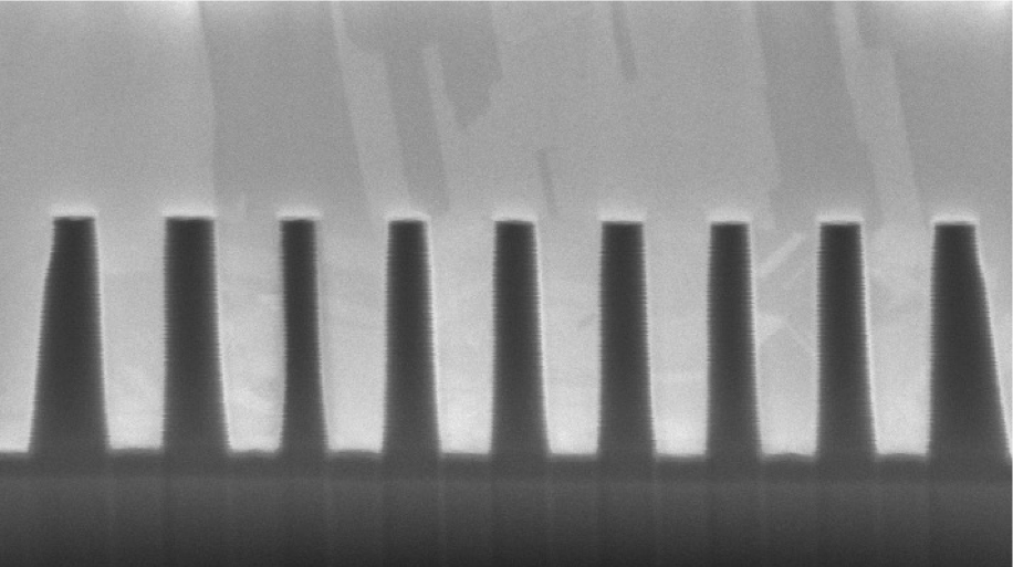
How do you know? We will cover this in more detail in the next article because it has a great deal to do with evaluating fill propagation. But suffice to say for now that you will be staring at FIB/SEM images.
What do you do? The two most likely causes for a failure in polarization are:
- Dwell time duration is wrong. A dwell step that is too long or too short can lead to a non-optimal adsorption profile. Too short may mean the accelerator did not have quite enough time to collect in the via bottom at high concentration. Too long may mean suppressor or leveler molecules had time to get down there too. The height of the via is going to be a factor here.
- Non-optimal mixture ratio of the organic components. Remember, suppressor and accelerator are in competition here. Too much of one and too little of the other and we don’t get the gradient we were aiming for. It’s important to note here that levelers are, in fact, a specific form of suppressor. And, in the case of the more advanced TSV fill chemistries on the market, the leveler is the more active than the conventional suppressor. So if you are using a more highly formulated TSV chemistry (you can tell by the price), adjusting leveler-to-accelerator ratios may be necessary.
Nucleation
As I hinted in the previous article, nucleation may or may not be necessary to good fill of TSVs. In my compelling cliff hanger on the topic, I also let drop that optimal nucleation can make up for some non-optimal outcomes from upstream processes.
What is nucleation? Nucleation has to do with the nature by which deposition of the copper initiates. And now we are talking about the molecular level, particularly way down at the via bottom. When the seed copper is rough, whether because of roughness in the seed copper itself or else roughness of the underlying layers translated through the seed, the texture will create hyper-local areas of increased current density. If you imagine zooming well in on the roughness, you will observe peaks and valleys in the surface. The peaks are the areas that generate the higher current density.
That higher current density more strongly attracts copper ions in the chemistry. The result is that copper ions can migrate to and preferentially deposit onto these peaks instead of distributing evenly. The peak thus increases in size, which makes that location even more favorable for deposition. And a bit of a runaway occurs. The observable result of this behavior is the formation of copper nodules. These nodules continue to grow faster than surrounding areas until the nodules begin to expand into each other. Guess what that causes. Yes. Voids. Large scale nodule formation will trap numerous tiny voids around the bottom side wall as the nodules grow into each other.
If such voids are observed, then better control of nucleation is likely necessary. The key here is that we not allow lazy copper ions to meander to whatever location they prefer, but rather to force them to lay down at the nearest location. We accomplish this by doing something that is very bad.
But it’s ok because we don’t do it for long. Agreed?
The bad thing we need to do is to put the system into a state approaching the “Limiting Current Density”. The limiting current density is the current density at which the ions available to react at the surface are consumed faster than they can be replenished. We do this by setting the current in the initial plating step to effect a much higher current density than normal. Perhaps 4 times higher. What happens is that we increase the deposition rate so much that copper ions do not have the chance to migrate but rather deposit as quickly as possible in the immediate vicinity, peak or no peak.
Again, this is a very bad thing we are doing and going on too long would cause a number of deleterious outcomes including…electrolysis of water.
I’ll bet you thought I was going to say voids.
Actually, the answer is also voids. It will cause voids.
So we would do this nucleation step for a short period of time, say 500 milliseconds. The result should be a “flattening” of the surface and the avoidance of nodule formation.
Maybe time to regroup:
- We wetted the features. Best way to do this is by using a vacuum prewet chamber, especially for TSVs with an aspect ratio of 5 or greater.
- We transferred the wafer to the plating reactor (ideally a fountain type that spins the wafer during plating) and performed an optimal entry which avoids trapping any air against the wafer surface.
- We allowed the wafer to dwell in the chemistry for a short period of time, allowing suppressor to coat the wafer surface and accelerator to race down into the vias ahead of everyone else. Then we initiated a potential on the system causing current to flow. A lovely gradient of adsorbed organic molecules formed on the via surfaces. Our vias were polarized.
- We had previously noted that roughness on the surface of the lower via was prone to causing nodules so we deployed the initial plating step as a high current nucleation step for half a second before returning to a normal current density.
- And now we are ready to look at propagation of fill.
Looking ahead to our final post on the topic, we have a lot of ground left to cover: Fill propagation, accelerator ejection and bulk layer plating. It all matters so now slowing down now. In fact, things are going to get quite fast now. Well, I mean in terms of plating steps that take an hour or so.
If you enjoyed this post, be sure to Like and to follow me so you don’t miss a single thing. Meanwhile, you suspect polarization didn’t work and you don’t want to wait til next week to get it under control. Get hold of us and let’s see how we can help your product or your fab retain technology sovereignty in a highly competitive marketplace.
Also Read:
Mastering Copper TSV Fill Part 1 of 3
Share this post via:


