KLA Debuts New Portfolio of Automotive Chip Testing Products – DBusiness
KLA Corp. a leading electronics equipment and service provider with headquarters in Milpitas, California, and locally in Ann Arbor, have launched four new products for automotive chip manufacturing.
“Today’s vehicles include thousands of semiconductor chips that sense surroundings, make driving decisions and control actions,” says Ahmad Khan, president of the semiconductor process control business unit at KLA. “These chips cannot fail, a fact that has led chipmakers to pursue new strategies to find and mitigate reliability-related defects in the fab, well before the chips are integrated in vehicles.”
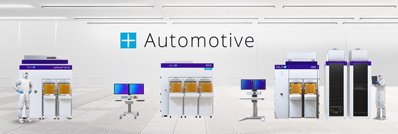
He says the new 8935 high productivity patterned wafer inspection system, the C205 broadband plasma patterned wafer inspection system, the Surfscan SP A2/A3 unpatterned wafer inspection systems, and I-PAT inline defect part average testing screening solution all work to ensure the chips going into increasingly electrified automobiles are reliable and meet strict quality standards.
“Tailored for fabs producing automotive chips, our new products detect potential reliability defects at the source and provide an innovative solution for inline screening,” Khan says. “These actions help fabs achieve production of high quality, high reliability chips at high yield to maximize their output.”
A wafer is a thin slice of semiconductor, such as a crystalline silicon, that is used for the manufacturing of integrated components.
The Surfscan SP A2/A3 unpatterned wafer inspectors incorporate deep ultraviolet optics and advanced algorithms to produce the sensitivity and speed required to identify and eliminate manufacturing defects that can cause automotive chip reliability issues.
The C205 patterned wafer inspector utilizes a broadband light source and NanoPoint technology to enable high-sensitivity discovery of critical defects. It is designed to be used in research and development and production ramping, it will increase the speed of new processes and devices.
The 8935 patterned wafer inspector employs new optical technologies and the DefectWise AI solution to capture a wide variety of critical defects at a low nuisance rate for fast and accurate identification.
I-PAT is an inline screening solution that runs on KLA inspection and data analytics systems. It begins by extracting defect characteristics from data collected for all wafers at critical process steps by the high speed 8 Series inspectors, including the 8935. I-PAT then leverages customized machine learning algorithms on the SPOT production platform and the statistical analysis capabilities of the Klarity defect management system to identify outlier defect populations so at-risk chips can be removed from the supply chain.
Khan says the three new inspectors form a complementary defect discovery, monitoring and control solution for larger design node chip manufacturing in the automotive industry.
“Our new products introduced today join our comprehensive portfolio of inspection, metrology, data analytics and process systems that support multiple parts of the automotive electronics ecosystem,” adds Oreste Donzella, executive vice president of the electronics, packaging, and components business unit at KLA. “Each one of these products plays a key role in ensuring high yield, reliability and performance of the chips, components, printed circuit boards and displays that comprise automotive electronics.”
![]()

