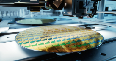
Khám phá các nguyên tắc cơ bản của quang khắc
In the semiconductor materials industry, photolithography is a crucial technology for creating intricate electronic circuits. Essentially, it’s the art of printing at the nanoscale level, enabling the precise patterning of semiconductor materials. The ability to do this well is important for companies in the industry because it determines how detailed and efficient microchips can be. This affects everything from our smartphones to medical devices. Even if you’re not an engineer, understanding the basics of photolithography opens a window into the fascinating world of micro- and nanotechnology that powers our everyday gadgets and shapes the future. Providing a fundamental overview of photolithography, we break down the process, explain the importance of photoresist materials, and explore some of the greatest innovations in photolithography, such as antireflective coatings.
What is lithography?
Lithography originates from two Greek words, lithos and graphia. Lithos means stones and graphia means to write, therefore lithography literally means writing on stones in Greek. However, in the industry of semiconductor lithography, also referred to as photolithography, our stones are silicon wafers.
Photolithography is the process that transfers shapes from a template to a surface using light. Photolithography, etching, and deposition techniques are used to build billions of transistors in today’s integrated circuits.
The fundamentals of lithography: Origins, and the impact it has on our industry throughout history.
What is a wafer?
Silicon wafers are created from a silicon ingot that is sliced using a diamond saw into thin wafers. Lapping makes the wafers uniform in diameter and round around the edges. They undergo etching to remove any remaining crystal damage and polishing to remove uneven surfaces. Doping changes the silicon electrical characteristics or other layers may be deposited to prepare for downstream processes.
There are many ways to perform polymer film deposition to coat a silicon wafer. Spin coating starts with a polymer being dissolved in solvent and then dispensed onto the center of the wafer while the wafer is being spun at high speeds. The spinning action spreads the material into a thin, uniform coating across the wafer.
The process of photolithography: A general imaging concept with process diagrams to visualize how the different steps and layers create designs specific to the application needs.
What is photoresist?
Photoresist is a light-sensitive coating that enables writing with patterned light onto an underlying silicon wafer. There are two types of photoresists: positive and negative.
With a positive photoresist, the light-sensitive layer becomes soluble when exposed to light. The photoresist is exposed to light patterned in a way that corresponds to the pattern desired on the wafer. Then the photoresist is exposed to a solvent to remove the soluble portions while leaving the unexposed portion, thereby revealing the pattern, similar to developing a photograph.
A negative photoresist is very similar except that the portion of the photoresist exposed to light becomes insoluble. Thus, when exposed to solvent after exposure to the patterned light, the portion of the photoresist that has been exposed to the light remains and the unexposed portions are removed.
Because the silicon wafer is reflective, there can be issues with interactions of the incoming light due to light reflecting off the wafer. Therefore, an antireflective coating is needed between the photoresist and the wafer.
The critical role of photoresist materials in the lithography process, providing some fundamental chemistry concepts and diagrams to illustrate the layers of materials.
What is the role of light in patterning?
The methods of illuminating silicon wafers have evolved to meet the changing demands in the industry.
Historically, the mask and photoresist would make direct contact. However, with the mass production of microchips, this poses an issue with cross contamination. Therefore, there was a shift to using a proximity lamination method where there was a gap, between 2 and 20 µm, between the mask and silicon wafer.
The demand to make chips faster and more efficient has led to projection photolithography. Projection requires an additional set of lenses to help with the reduction of the light source between the mask and the photoresist.
The role of light in the lithography process by providing context of different exposure methods and sources of light.
What is an antireflective coating?
During the photolithography process, if the light patterning bounces off the reflective surface of the silicon wafer, it will interact with the incoming light, resulting in an interference pattern called a standing wave. The standing wave will create an undesirable wave profile along the walls of the exposed photoresists. This is even more problematic when forming overlying patterns on top of existing structures.
Bottom antireflective coatings (BARCs) reduce reflection by being inherently absorbing and by introducing a phase-shifted light that destructively interferes with incoming light incident on the wafer at the bottom of the photoresist.
Antireflective coatings are a necessary part of the photolithography process for modern chip technology. This video illustrates the role antireflective coatings have in the processing of light through patterns and the impact it has on underlayers.
Understanding photolithography fundamentals provides crucial insights into a foundational technology within the semiconductor materials industry. By tracing the origins of lithography and examining key processes like photolithography, etching, and deposition techniques, we gain a deeper understanding of semiconductor circuit fabrication and the materials that enable success.
Essential components such as photoresist materials and antireflective coatings have a pivotal role in enabling precise nanoscale patterning. Whether you’re an experienced industry professional or an aspiring engineer, grasping the basics of photolithography unveils the profound impact of micro- and nanotechnology on modern technology. As innovations in projection methods and advanced illumination techniques drive chip manufacturing forward, lithography continues to lead the way in semiconductor technology, fostering progress and innovation in the digital era.


