Intel và Cadence hợp tác để thúc đẩy tiêu chuẩn UCIe quan trọng nhất

The Universal Chiplet Interconnect Express™ (UCIe™) 1.0 specification was announced in early 2022 and a UCIe 1.1 update was released on August 8, 2023. This open standard facilitates the heterogeneous integration of die-to-die link interconnects within the same package. This is a fancy way of saying the standard opens the door to true multi-die design, sourced from an open ecosystem that can be trusted and validated. This standard is very important to the future of semiconductor system design. It’s also quite complex and presents many technical hurdles to practical usage by many. Intel and Cadence recently published a white paper that details how the two companies are working together to get to the promised land of a chiplet ecosystem. If multi-die design is in your future, you will want to get your own copy. A link is coming, but let’s first examine some history and innovation as Intel and Cadence collaborate to advance the all-important UCIe standard.
Some History
It turns out Cadence and Intel have a history of collaborating to bring emerging standards into the mainstream. In 2021, the companies collaborated on simulation interoperability between an Intel host and Cadence IP for the Compute Express Link™ (CXL™) 2.0 specification. Like UCIe, this work aimed to have a substantial impact on chip and system design.
The specification, along with the latest PCI Express® (PCIe®) 5.0 specification provided a path to high-bandwidth, cache-coherent, low-latency transport for many high-bandwidth applications such as artificial intelligence, machine learning, and hyperscale applications, with specific use cases in newer memory architectures such as disaggregated and persistent memories.
The ecosystem to support this standard was rapidly evolving. Design IP, verification IP, protocol analyzers, and test equipment were all advancing simultaneously. This situation could lead to design issues not being discovered until prototype chips became available for interoperability testing. Finding the problem this late in the process would delay product introduction for sure.
So, Intel and Cadence collaborated on interoperability testing through co-simulation as the first proof point to successfully run complex cache coherent flows. This “shift-left” approach demonstrated the ability to confidently build host and device IP, while also providing essential feedback to the CXL standards body.
You can read about this project here.
Addressing Present Day Challenges
In 2023 Cadence and Intel began collaborating again, this time to advance the UCIe standard and help achieve on-package integration of chiplets from different foundries and process nodes – the promise of an open chiplet ecosystem. UCIe is expected to enable power-efficient and low-latency chiplet solutions as heterogeneous disaggregation of SoCs becomes mainstream. This work is critical to keep the exponential complexity growth of Moore’s Law alive and well. Monolithic strategies won’t be enough.
To achieve a chiplet ecosystem, design IP, verification IP, and testing practices for compliance will be needed, and that is the focus of the work summarized in this white paper. Here are the topics covered in the white paper – a link is coming so you can get the whole story.
UCIe Compliance Challenges. Topics include the electrical, mechanical, die-to-die adapter, protocol layer, physical layer, and integration of the golden die link to the vendor device under test. The PHY electrical and adapter compliances include the die-to-die high-speed interface as well as the RDI and FDI interface. The mechanical compliance of the channel is tightly coupled with the type of reference package used for integration. There are a lot of technical challenges and design-specific challenges discussed in this section.
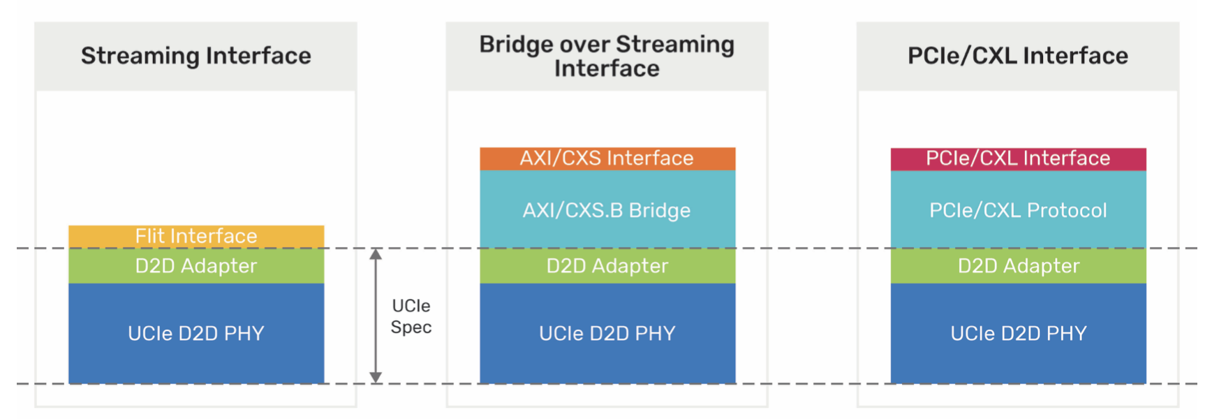
The Role of Pre-Silicon Interoperability. There are many parts to each of the standards involved in multi-die design. The entire system is designed concurrently, resulting in all layers going through design and debug at the same time. Like the work done on CXL, “shift-left” strategies are explored here to allow testing and validation to be done before fabrication. The figure below illustrates the relation of the various specifications.

UCIe Verification Challenges. Some of the unique challenges to the verification environment are discussed here. Topics covered include:
- D2C (data-to-clk) Point Testing
- PLL Programming Time
- Length of D2C Eye Sweep Test
- Number of D2C Eye Sweep Tests
UCIe Simulation Logistics. For this project, the Cadence UCIe advanced package PHY model with x64 lanes was used for pre-silicon verification with Intel’s UCIe vectors. Topics covered include:
- Initial Interoperability
- Simulation – Interoperability over UCIe
- Controller Simulation Interoperability
The piece concludes with UCIe Benefits to the Wider Community.
To Learn More
If multi-die design is in your future, you need to understand the UCIe standard. And more importantly, you need to know what strategies exist for early interoperability validation. The white paper from Cadence and Intel is a must read. You can get your copy here. And that’s how Intel and Cadence collaborate to advance the all-important UCIe standard.
Also Read:
Overcoming Verification Challenges of SPI NAND Flash Octal DDR
The Impact of UCIe on Chiplet Design: Lowering Barriers and Driving Innovation
The Future of Logic Equivalence Checking
Share this post via:


