Intel says latest breakthroughs in chip design promise more of Moore's Law – FierceElectronics
As AI and other advanced technologies expand the need for accelerated compute, chip designers are finding ways to cram more components inside processors, partly so that circuit boards inside servers and laptops don’t threaten to expand beyond their enclosures.
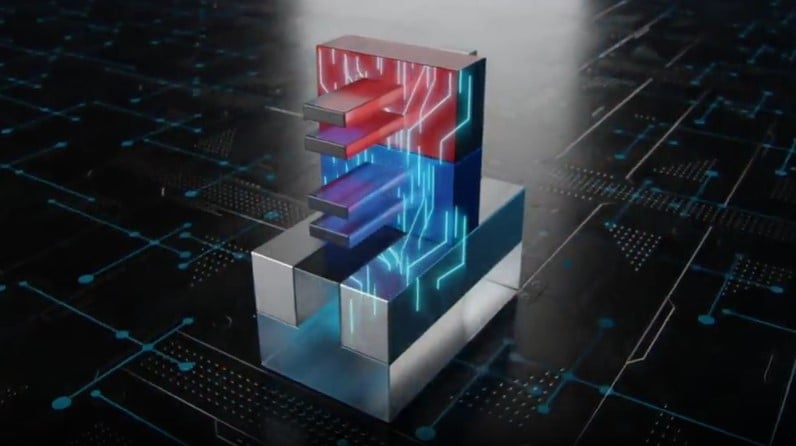
In one example of ongoing work, Intel researchers showed off 3D stacked CMOS transistors combined with backside power and direct backside contact at a technical event on Saturday.
The company claimed the first-of-its-kind advancement will help continue the evolution of Moore’s Law to scale to ever-higher performance in future semiconductors.
“Continued innovation is more critical than ever,” said Sanjay Natarajan, Intel’s general manager of components research, in a statement timed with IEDM (IEEE International Electron Devices Meeting). Intel is forecasting five chip nodes in four years and needs new chip architectures to move to what Intel calls the Angstrom Era. That’s when some physical features inside chips can no longer be accurately measured, as today, in nanometers, or billionths of a meter. With angstroms, physical features are one ten-billionth of a meter.
Intel set a goal one year ago to extend Moore’s Law to 1 trillion transistors on a single processor package by 2030. That was roughly 10 times the highest number on a microchip at the time. Moore’s Law says the speed and capabilities of computers are expected to double every two years as the number of transistors on a microchip increases.
On Saturday, Intel experts showcased 3D stacked CMOS (complementary metal oxide semiconductor) transistors along with backside power and backside contact. What that means is that Intel showed the ability to vertically stack complementary field effect transistors at a scaled gate pitch down to 60 nm, a process allowing area efficiency– similar to how a two- or three-story house can offer more square footage while using up less of the area in a lot.
Backside power and direct backside contacts simply means the power-delivery interconnects (or wires) to a processor are moved to beneath the silicon to leave more room for data interconnects above the silicon. Also the power interconnects can be made larger and therefore less resistive.
Vertical stacking and backside power shows the company is leading in the science of gate-all-around transistors, Intel claimed in a release, “putting it ahead of the competition.”
Intel’s first implementation of backside power delivery is expected to reach manufacturing in 2024 through what it calls PowerVia. Researchers are now looking at other processes to go beyond PowerVia.
Intel also successfully demonstrated large-scale 3D monolithic integration of silicon transistors with gallium nitride transistors on the same 300 mm wafer instead of on each semiconductor package. The integration is called DrGaN, or Driver-GaN Power Switch.
RELATED: CES 2024 previews with, what else?—AI, then more AI and Intel and AI
