Intel GenAI For Yield, TSMC CFET & 3D Stacking, AMD 3D Device Modeling, Applied Materials Material Innovation, SK Hynix HBM4, Micron 3D DRAM & FeRAM, Hybrid Bonding so với TCB – IEDM 2023
Gordon Moore’s spirit lives on as the industry keeps chasing smaller, denser, cheaper, and faster semiconductor devices. The premiere place to hear about these developments is the International Electron Devices Meeting (IEDM), and today we want to do a roundup of this year’s developments for the future of semiconductor device scaling. For those who missed last year, we covered many important topics.

What themes did we hear most about at IEDM this year?
We’ll cover a few of the topics where AI was more than just a buzzword (although it was often a buzzword), including Intel’s innovative work on using diffusion models to improve process yields.
The primary topics covered will be advanced logic review of advances for beyond 2nm from TSMC, Intel, and Samsung regarding 2D materials, CFETs, and backside power delivery. Applied Materials showed off their new suite for metal interconnects on 2nm and beyond, which could drive share gains.
The other most exciting area was with memory. Micron presented a non-volatile FeRAM that is denser than the worlds densest DRAM and within an order of magnitude in performance. China’s leading DRAM firm, CXMT openly flaunted their violation of multiple export controls.
SK Hynix showed off their plans for HBM4 hybrid bonding versus flipchip MR-MUF versus TCB, Samsung’s road to >1,000 layer NAND with multiple forms of wafer stacking, Kioxia presenting the world’s densest high volume production grade NAND and their CBA approach.
We will also cover Intel DrGAN, IBM’s Future of EUV which confirms elements of our report from last month on High-NA’s lack of competitiveness medium term due to dose issues, and a humorous award we will start giving out at SemiAnalysis to presenters at technical conferences.
Intel showed early work on a deep generative model for predicting device variation. Every generation the complexity of chips grows far more than the transistor counts, and the number of Cadence emulation/simulation boxes continues to explode. Nvidia is trying to bring GPUs to improve this flow.
Existing EDA benefit from a virtuous cycle where increased compute power enables better modeling which enables the production of further increased compute power. In a sense it’s the same as the generative AI scaling laws, although currently far more tame. Utilizing AI to design better AI accelerator chips is rapidly occurring with Nvidia and Google far ahead of the pack. Nvidia’s operation lightspeed is largely possible due to these advances.
Bringing generative AI to process and device modeling is an obvious first step because it is an extremely data intensive task that has large, high quality (relative to other applications) dataset readily available to chipmakers. The benefit of higher process yields and faster cycle times are easily quantifiable and translated to revenue.
While still early in development, Intel presented promising results from implementing GenAI models for this. Initial testing was performed with 2 different model types: generative adversarial networks (GAN) and diffusion model.
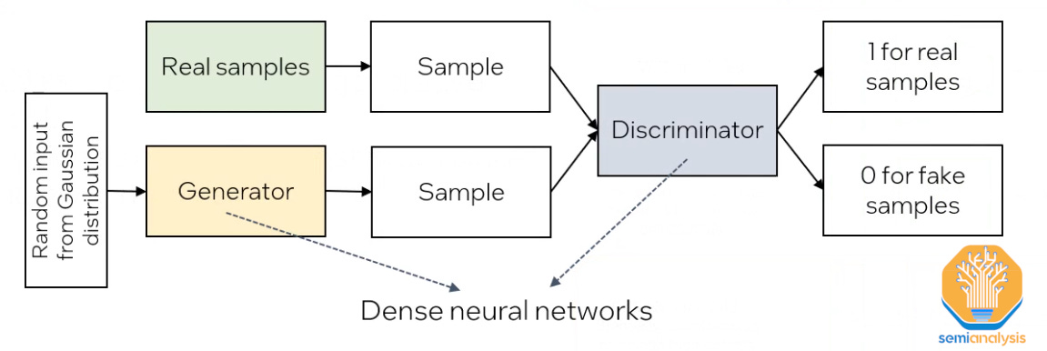
GAN models are a popular architecture commonly used in image, text, and audio generators that require synthetic samples that closely resemble real ones. They comprise 2 deep neural networks: generator and discriminator. The generator creates fake samples from random noise. These fake samples are input along with real samples to the discriminator, which attempts to discern real from fake. In essence the generator is trying to fool the discriminator, hence the adversarial part of generative adversarial network.
Through training, the quality of generator output samples will approach or even be indistinguishable from real. GAN models, however, are prone to mode collapse. This means their output fails to replicate the entire space of the input distribution function; in simple terms it means the outputs will tend to look similar. While this isn’t an issue for many popular consumer applications like image generation, it is not viable for chip design and process modeling.
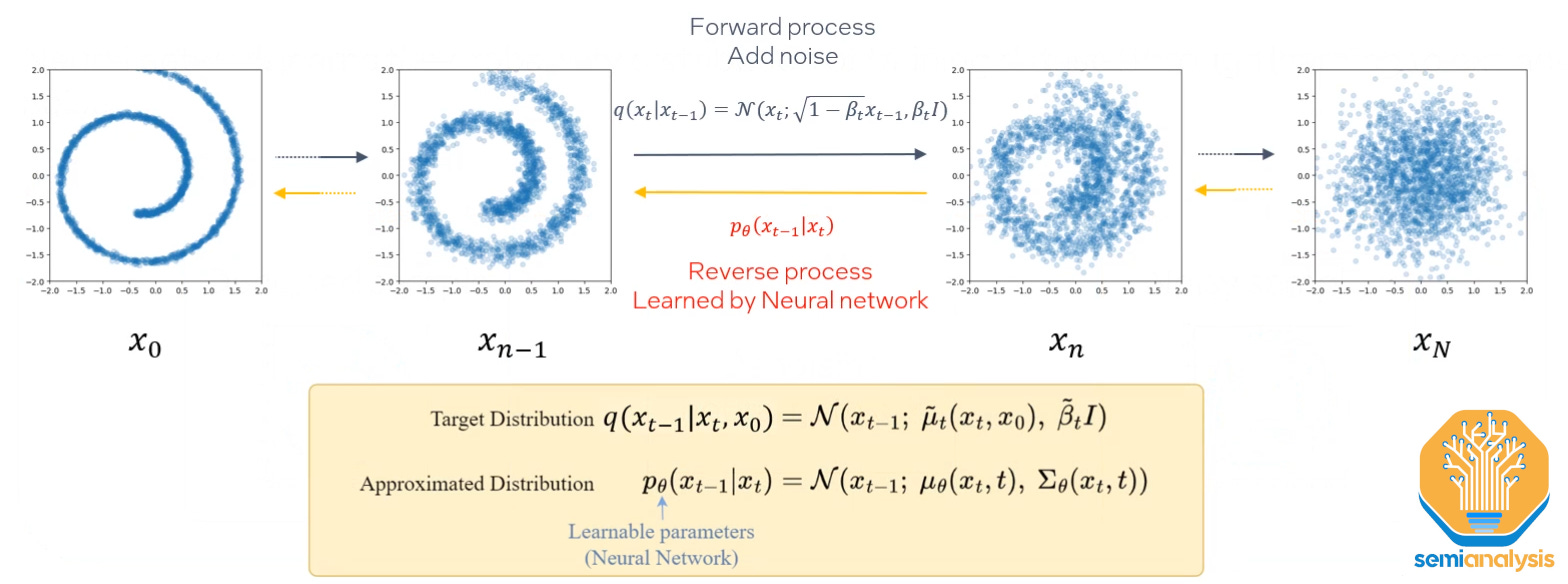
The critical difference is that, in this model setup, process yield is defined by the long tails of the distribution – so failing to replicate those means the model is not correctly predicting yield.

Diffusion networks are much better suited to the task. Real samples with added noise are used to train the model, which learns to denoise them. Crucially, diffusion networks in this application were able to replicate the long tails of the sample data distribution, thus providing accurate predictions of process yield.
In Intel’s research, SPICE parameters, used in the design phase as part of device simulation, are used as input for the deep learning model. Its output is the predicted electrical characteristics of the device as manufactured, or ETEST metrics. And the results show the model is capable of correctly predicting the distribution of ETEST metrics. Circuit yield is defined by the tails of this distribution. So, by correctly predicting the distribution of ETEST metrics, the model is correctly predicting yield.
The potential here is clear: better optimization of chip yields at the design stage means lower costs. Fewer mask respins, shorter development times, and ultimately higher yield would all be strong differentiators for foundries and design teams that can implement models into their PDK/design flows.

Current work is in the research stage but expect that all major foundries and design firms will be working to industrialize techniques similar to this. This base data is closely guarded, so it is really tough for a startup or even fabless design firm to get access to everything. In that sense, Intel as an IDM is advantaged. If one can get the data, it is the perfect place for an entrepreneur to start a firm. We’d definitely do angel/seed here.
Logic scaling has been the beating heart of the industry for many years. While the recent pace of scaling has slowed, it remains one of the key drivers behind continued improvements in the economics of semiconductors. IEDM is traditionally a place for chipmakers to show progress towards realizing their process roadmaps. We are going to dive right in, so if you need to catchup to where we are at a higher level, read the future of the transistor here.

Current development work is focused in 2 areas: traditional horizontal scaling in the x and y direction, and 3D stacking (z direction).
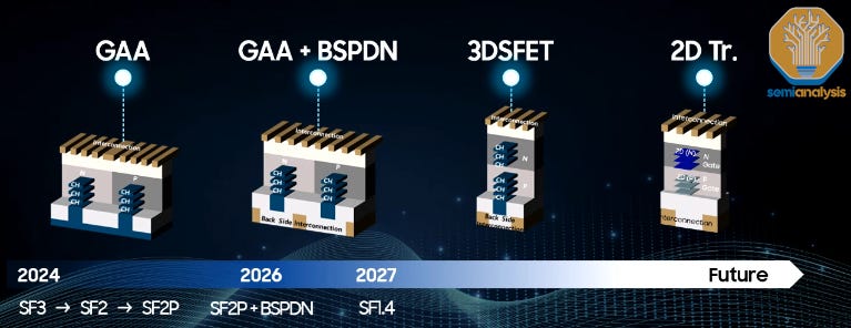
For horizontal scaling, gate-all-around (GAA) is going to enable shrinking to continue with “2nm” class nodes just as FinFET is losing steam. These 2nm class nodes will enter high volume manufacturing at Intel and TSMC in 2025. Samsung’s 3nm has gate-all around transistors as well, but despite claims of high volume manufacturing, they still have not shipped any fully functional chips, even in their own smartphones.
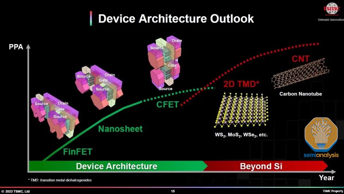
There were many new developments are focused on further shrinking the GAA architectures as current materials will run out of steam near the end of the decade. This will require turning to exotic “2D” materials – first transition metal dichalcogenide (TMD) monolayers, then possibly carbon nanotubes.
In the vertical direction, the first stacked transistor architectures are coming to fruition. We’ll go into greater detail on each of these ideas as we cover updates from TSMC, Intel, and Samsung.
2D channel materials are expected to be one of the next evolutionary steps in GAA architecture. Initially, GAA processes will use silicon (Si) channels, same as traditional finFETs. However, as contact resistance and parasitic capacitance of Si channels increases at smaller scales, new materials with better electrical performance will be required to continue scaling. This transition may be necessary as soon as the 10A (1nm) node, roughly in the 2030 timeframe.
TMD monolayers, colloquially “2D materials”, since they are only a few atoms thick, have long been known to have the required properties; as development moves towards industrializing a process to fabricate 2D materials, chipmakers appear to have converged on the TMDs. No, it’s not carbon nanotubes, often thought of as a holy grail, but rather, MoS2 for N-type metal-oxide semiconductors (NMOS) and WSe2 for P-type metal-oxide (PMOS) devices.
Being just a few atoms thick, these materials are of course challenging to fabricate, and the race is on to find reliable methods of producing them at scale. Last year, we discussed the debate of material growth vs transfer in detail, but it seems everyone is converging on growth as transfer has some very difficult challenges.
TSMC demonstrated working nanosheet FETs (NSFETs) fabricated with a single nanosheet channel. The ability to construct 2 stacked nanosheets was also shown but without mention of any working transistors built on those nanosheets. A key point was that the 2D material was grown directly via chemical vapor deposition (CVD) rather than utilizing an additional film transfer step as had previously been done.
Growth is the fundamental problem for 2D materials. No solution exists today that can reliably grow 2D materials over a non-negligible surface area.


TSMC also showcased a novel “c-shaped” contact scheme, a method for reducing contact resistance (lower contact resistance means better device performance) as the “c” shape of the contact surrounds the channel, providing greater contact area and thus lower resistance.
Where TSMC detailed only an NMOS device, Intel demonstrated working PMOS and NMOS devices with TMD channels. Furthermore, Intel fabricated these devices on a 300mm wafer pilot line, not just at lab scale. At least in terms of research presented, Intel was way ahead of TSMC on the race to 2D materials. However, it is important to note that these were simple planar transistors, did not utilize the GAA architecture, and were not fabricated at a pitch that will be needed for the 14A+ node due in a handful years.
Samsung, surprisingly, made very little noise about 2D materials. Dr. Choi, president & GM of Samsung’s Foundry Business, mentioned the possibility of 2D channel materials extending GAA scaling, but no technical papers were presented on the topic. Despite being “first movers” for GAA, they appear to be letting others do the pathfinding on 2D.
Oddly based on the presentations at IEDM, it seemed Samsung still hasn’t figured out which of the 3 different types of back side power delivery schemes they want to do while Intel and TSMC clearly have decided their roadmap.
Regardless of the advancements being made, currently we are in the long tail of horizontal scaling: each step brings less benefit while taking longer to develop than the one before. 3D stacking is just the opposite – a novel technique with potential for 1.5-2x density scaling in the first generation alone.
Traditionally, chips comprise 1 layer of both NMOS and PMOS with the necessary connections to and between them built atop. Advances in fabrication techniques and the necessity to look beyond horizontal scaling mean that building multiple layers of transistors atop one another is becoming possible.
The first natural step will be stacking 1 NMOS + 1 PMOS transistor, the reason being that together they can be connected to form an inverter, or NOT gate, a fundamental building block of digital circuits. More complex standard cells will be very difficult to produce as well. TSMC published a nice illustration of the concept, along with a composite of transmission electron microscopy (TEM) images showing the real thing.


Last year, most of the work in this area was shown by university labs. This year, all major logic players (along with IMEC) showed results led by their internal R&D organizations, a sure step towards commercialization. 3D stacking is likely to be rolled out around the 10A node, around the 2030 timeframe.
In general, the 4 approaches seem to be converging in terms of architectural decisions and fabrication schemes.

Intel’s integration scheme was particularly interesting and worth highlighting as it showed not just CFETs, but also backside power delivery with backside contacts for NMOS and backside power delivery with PowerVia for the PMOS. The power delivery problem becomes incredibly hard with CFET.
One key area to watch in the future will be thermal performance. We saw more than one chipmaker paper on scaling enablers (3D transistor stacking, backside power delivery, advanced packaging, etc.) that claimed no regression in thermal performance. AMD presented a paper that made it very clear from a customer perspective that thermal issues need extra attention.

AMD’s simulations suggest up to a 5% performance decrease when using backside power delivery because the chip must be throttled to avoid overheating. The main culprit was the wafer thinning and bonding process. While required to fabricate backside devices, it has the unfortunate side effect of strongly reducing the thermal conductivity of the silicon near the devices, meaning the device cannot dissipate heat as effectively.
3D packaging encountered the same issues in cases where bulk wafer thinning was required: a performance loss of up to 5% due to throttling at hot spots.

Note that logic scaling may exacerbate this problem since it has a compounding effect on heat generation. Not only does electrical resistance increase as devices shrink, thus increasing heat generation, but transistor density increases as well, so the heat generated in a given area is higher. Dennard scaling broke down quite a while back, but it’s increasingly becoming a problem with each shrink. Further scaling techniques such as CFET, 3D Stacking, and backside power delivery are exacerbating these issues.
This result has a few interesting implications. First, chip design flows must start treating these as “1st class problems,” with tooling that allows designers to mitigate them. Second, fabrication methods should also be addressing thermal challenges. Currently the EDA tooling provided by Cadence and Synopsys lack here according to multiple designers we have spoken with.
We saw only one paper focused on the latter topic of combatting runaway thermal density with normal 3D stacking via advanced packaging, and it may be the perfect solution to the issues AMD showed. TSMC showed 2 approaches to dealing with these increased power densities, both attempting to increase the thermal conductivity at wafer-to-wafer bonds where the thinned silicon has poor performance.
First, was placing dummy copper thermal vias – essentially small “heat pipes” to conduct heat away from hotspots. This showed excellent thermal performance, but because copper also conducts electricity as well, this approach negatively affected electrical performance despite not being hooked into the signal interconnects.
Second and more promising was using thermally conductive layers between bonded wafers. Currently when wafers are bonded with a SiO2 bond between them. Replacing this with a high thermal conductivity material was shown to improve thermals without the adverse electrical effects.

The benefits are clear, but these thermally conductive materials not easy to produce. Two candidate materials were shown: AlN and diamond. TSMC demonstrated both in a lab setting, produced to a sub-micron thickness with high enough thermal conductivity to be viable.


While this process does not appear to be industrialized, it is worth watching given the problems detailed above. We thought it was very notable that there was not more attention given to it at the conference, perhaps more attention will be given to this at ISSCC or VLSI.

From a fabrication standpoint, it may make sense to replace pure fusion bonds such as those in back side power delivery, first, rather than those in hybrid bonding, where bonding issues may arise.
While device scaling seems to receive the bulk of everyone’s attention, back-end-of-line (BEOL) scaling is just as, if not more important. Increasing transistor density is of no use if signals and power cannot be effectively routed to them. One of the biggest challenges is translating theoretical transistor density increases into routed density increases on actual devices.
A key challenge in scaling these interconnects is the increasing resistance as the “wires” shrink. In fact, this challenge can wreck an entire process node: Intel’s long struggle with the 10nm node was in large part due to an attempted switch away from copper to cobalt interconnects on the lowest metal layers. While cobalt has lower resistance than the traditional copper at that pitch, there were so many issues in implementation that the choice was eventually walked back.
Getting back-end-of line scaling design decisions wrong can be massively value destructive for chipmakers. New interconnect materials and fabrication schemes are therefore worth paying attention to.
Applied Materials and IMEC both showed their solutions for scaling interconnects. Applied Materials in 2022 debuted a titanium nitride liner + tungsten fill to create smaller, lower resistance interconnects. This year they noted that this process is now in high volume manufacturing at a major logic manufacturer. Building on that, Applied Materials debuted an all-tungsten interconnect scheme that promises further scaling capabilities.
The presentation was clearly technical marketing, but the TSMC and Intel folks in the room were paying extremely close attention and asked very good questions.


Notably, this scheme can be accomplished in-situ with Applied Materials’ Endura tool, meaning that the wafers are never exposed to the fab environment while building up the interconnects. Oxygen exposure causes performance-degrading due to oxidation of the interconnects, so maintaining the same vacuum throughout means much better results: >20% lower resistance than an ex-situ process.
Applied Materials can bundle many tools of a single process module in a way others cannot, which gives them room to take share from other etch, clean, and deposition providers on the early layers of the back end of line, IE, one the most costly parts of wafer fabrication.
Memory needs for both compute and storage in the AI era are exploding. There is a tremendous memory wall which is limiting advancements. Micron noted in a plenary session that data growth is accelerating on a similar trajectory to compute needs, with both slopes getting steeper.

And just as in logic, memory scaling will need to continue in order to meet growing data needs in an economic fashion. Doing so requires advances in many areas. The logic used to control memory arrays will need to scale accordingly, and FinFETs are on the roadmap near the end of the decade.

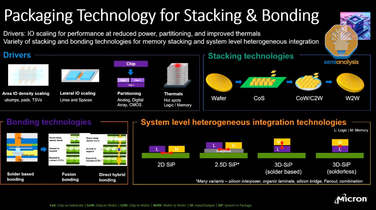
Packaging technology will also play a part, as denser integration of memory and compute enables better system-level performance (we won’t dive too deeply into packaging here; see our advanced packaging deep dive and look for more from us on this topic soon).
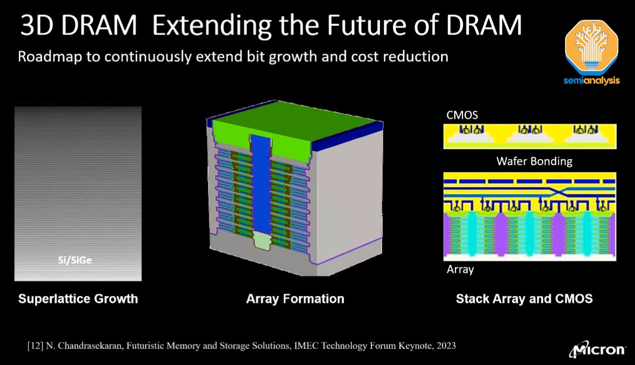
Finally, there is the memory array itself, where the key inflection point is 3D DRAM insertion. Some background is necessary here: traditionally, DRAM memory arrays consist of vertical capacitors. As with transistors and logic, memory scaling has largely been accomplished by simply making the devices ever smaller. DRAM capacitors are generally tall, narrow cylinders. Reducing their diameter allows them to be packed together in higher density but means they must be taller to maintain enough capacitance – in other words their aspect ratio must increase.
Today’s DRAM arrays have extremely high aspect ratios and are very challenging to fabricate in much the same way that horizontal scaling is reaching physical limits for logic. Producing these is primarily an issue with maintaining uniformity as you shrink horizontally and aspect ratios continue to grow.
At some point in the future, scaling will require 3D DRAM. The concept is simple: if the capacitors cannot be made any smaller/taller, make them horizontal instead and stack large numbers atop each other.


The importance of this shift is the difference in fabrication methods. Relative to existing planar DRAM, 3D may require 50% less lithography use and a large increase in etch and deposition tools. A similar rebalancing occurred in the transition from 2D to 3D NAND memory and will have strong effects on the DRAM equipment supply chain – a ~$30B market when the memory cycle peaks again in 2025.
The key, then, is when the transition will occur. Micron’s plenary presenter called it “the quintessential question,” and the answer given was a heavily caveated version of “within 10 years.” It’s very telling that none of the major memory manufacturers will be presenting serious 3D DRAM papers at IEDM because this is a race that will shift market share. This year there were a few on the topic from Macronix, but none from Samsung, SK Hynix, or Micron. An example roadmap from IMEC shared by Micron shows a vague timeline between 2030-2035. In other words, not expected in the short term.

Memory is one the most important scaling vectors for achieving civilization redefining AI technologies, and China is investing heavily in leapfrogging the rest of the world with these technologies and has already started implementing LLMs for propaganda / electoral subversion as well as within the PLA.
Much like with how Huawei openly released their 7nm mobile chip, the Kirin 9000S, as Gina Raimondo, was in China, CXMT also surprised us by candidly announcing their violation U.S. export controls at IEDM in San Francisco. CXMT presented their Gate-All-Around Vertical Transistors manufactured at the 18nm half pitch.

CXMT violated two different portions of the US export controls. US tools can not be shipped to firms that fabricate 18nm half pitch DRAM devices. US tools cannot be shipped to firms that fabricate gate all around transistors. CXMT has done both of these simultaneously in a functional device. With the way the law is written, American tool makers such as Applied Materials, Lam Research, KLA, and Onto can now no longer ship tools to the facility at which CXMT fabricated these devices. While the device above is production for research purposes with mass volume coming later, the regulations do not discount it. CXMT only has 1 fab site currently.
Our wafer fabrication equipment model and supply chain sources point to CXMT having 7 billion dollars of equipment spending for DRAM production next year, with 3.8 billion of that going to American tool firms and Applied Materials as the largest contributor at $1.8 billion of shipments to CXMT in 2024. This spend is higher than Micron for DRAM because of the recent $5B injection into CXMT’s government backed joint venture, Changxin Xinqiao, from federal and local governments.
While CXMT is still a few years behind on process technology for high volume production DRAM, they are only a year behind on most commercial forms of DRAM. We also expect their HBM3E for AI to ship in mid-2025.
Enforcement of these rulings may continue to fail, but with the way the regulations are currently written, CXMT has said that all US tool firms are in violation by continuing to ship to CXMT. This is why it is surprising that they admitted to doing so in public. To be clear, it is not shocking that they were able to exceed the limits. We even called out CXMT specifically in our piece on the failed U.S. sanctions.
SK Hynix gave multiple presentations on HBM packaging. This included the most comprehensive overview of their MR-MUF technology, which we covered in our prior HBM and CoWoS deep dives. To recap MR-MUF stands for Mass Reflow – Molded Underfill which SK Hynix adopted with HBM2E after using the TC-NCF (Thermo Compression – Non-Conductive Film).
As the name implies MR-MUF uses a traditional flip-chip mass-reflow process to stack the die and form the joints. This is much higher throughput as it is a batch process (solder reflow is performed once for the entire stack) compared to TCB which requires an individual bond process for each layer on the stack.
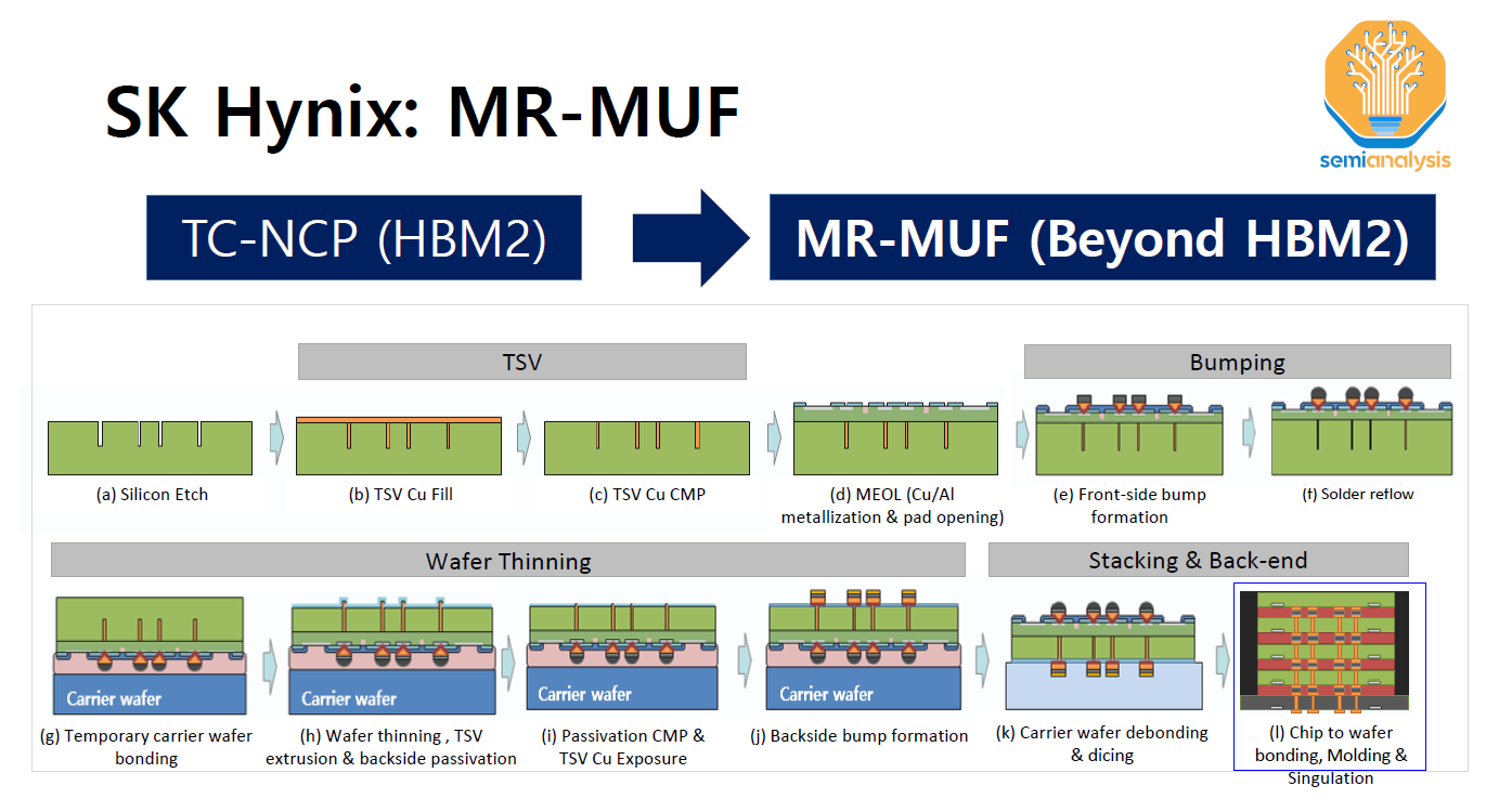
It is not just productivity, but MR-MUF results in more performant HBM. In between the die an epoxy molding compound is used as the gapfill material which has much higher thermal conductivity than the non-conductive film in TC-NCF. This results in lower junction temperatures and is a significant benefit to customers given the importance of managing thermals for high power chips like GPUs.

Hynix went deeper into some of the challenges with MR-MUF and, so far Hynix is the only supplier to have overcome these. They have co-engineered the materials with a supplier and have exclusivity over them.
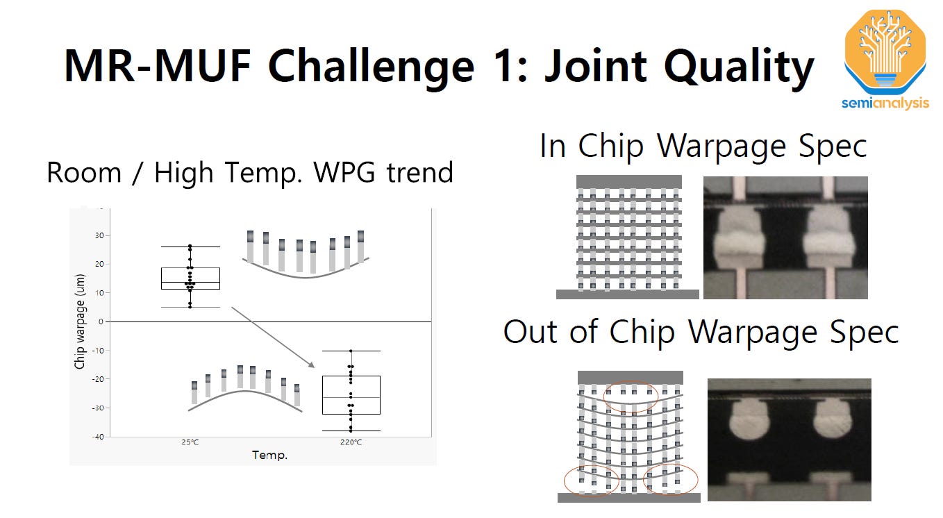
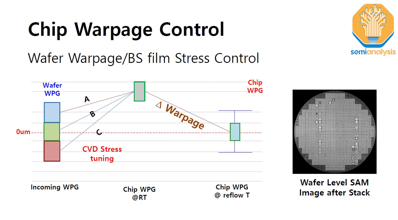
First is the challenge of controlling die warpage: especially with a high free-standing stack of very thin die. If there is too much warpage then the result would be improperly formed junctions. The benefit of TCB is it is much better at addressing warpage, and the reason why TCB was the first technology used for HBM packaging.
It’s also why Intel is unique in using TCB far more commonly in packaging versus the rest of the OSAT and foundry packaging ecosystem. Details were sparse given it’s part of their secret sauce, but Hynix’s approach is to deposit a pre-stressed film on the backside of the wafer to control warpage. Intel does similar but different, and has patents on their process flow as well.
The other challenge is dispensing the EMC to fill the gaps between the die and ensuring there are no voids. The role of the underfill is to provide structural support for the bumps but voids in the underfill reduce this support. The denser bumps and narrow gaps make the underfill dispense more challenging for HBM.
To address this, Hynix has optimized the mold tool and found that the pattern of the EMC dispense is also critical. It was found that using a chip face up mold tool resulted in unavoidable voids so a custom face down mold tool must be used. Also certain dispense patterns result in lower voids like the Serpentine Imp.2 pattern on the far right in the exhibit. Another thing is to ensure the EMC is not placed between the stacks, which reduces airflow, resulting in trapped air in the structure that results in voids.
There was also importantly a discussion on the HBM4 roadmaps from SK Hynix.
The rest of this report will cover SK Hynix thoughts on HBM4 hybrid bonding versus flipchip/TCB, Micron’s impressive non-volatile FeRAM that is denser than DRAM and in the same ball park for performance, Samsung’s road to >1,000 layer NAND, Kioxia presenting the world’s densest high volume production grade NAND and their CBA approach.
It will also cover non-memory topics such as Intel DrGAN, IBM’s Future of EUV which confirms elements of our report from last month on High-NA’s lack of competitiveness near term, and a humorous award we will start giving out at SemiAnalysis to presenters at technical conferences.
