Intel có quay lại không? Đo lường sự hồi sinh của xưởng đúc và sản phẩm
Before Pat Gelsinger took over Intel as CEO, the company spent over a decade in a slow descent due to a focus on financial engineering. The decline was set in motion by the then CEO, Paul Otellini, who made the shortsighted decision to turn down the iPhone contract due to apprehension over margins. The main concern was that Apple’s customization demands would be costly and would be amortized over low volume projections that turned out to be woefully underestimated by Intel. This led to Intel missing out on the last decade’s largest area of growth: mobile.

The loss of mobile fed most leading-edge volume growth to competitors which in turn propelled R&D and high-volume manufacturing (HVM) learnings for the ex-Intel ecosystem. While Intel’s road to irrelevance was paved with many more blunders, this was just the beginning of the end. Fast forward to today, and Intel’s financial situation is quite dire, with negative free cashflow and large net losses in quite a few quarters in 2022 and 2023. Furthermore, Intel continues to lose market share in most of their major product segments. In the Datacenter segment, the former cash printing machine, the situation is particularly dire as share losses will continue till next year at minimum. If nothing changes, it’s game over.
Thankfully, the era of complacency at Intel is over, and they have now recognized many of their pitfalls. Intel is now attempting to building a world-class systems foundry. That’s different from a traditional wafer foundry business of only making the best process technology. Instead, Intel wants to make the best technology at every layer of the stack and make it available to anyone. System level engineering is far more important in the AI era as shown by Google’s TPU and Nvidia’s GB200 rack. To be clear, the jury is still out on whether Intel can execute on these ambitious plans. Nvidia, AMD, Broadcom, TSMC, and the hyperscalers are all beating Intel at each of their core competencies and beating or partnering with these firms is not going to be easy.
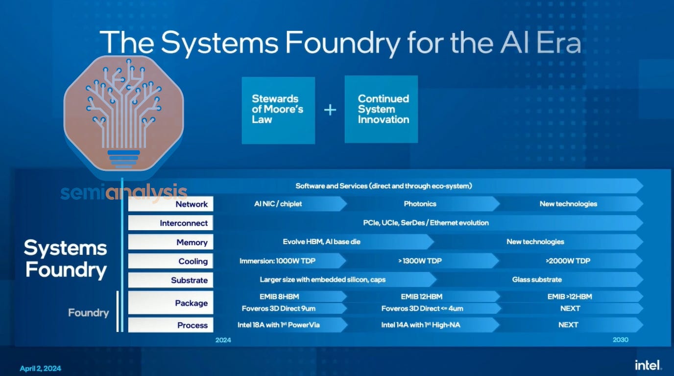
The systems foundry approach is quite important as Intel wants to be able to provide everything from leading edge process nodes to hybrid bonding to EMIB to large format packages to advanced cooling solutions to HBM base dies / buffer to leading connectivity IP including die to die adapters and SerDes. Intel even wants to offer NICs as chiplets to third party vendors! Their IP war chest will be opened to those wanting to use the systems foundry, and the pricing will be quite attractive versus existing merchant only solutions.
Today we’ll cover Intel’s restructuring of the company, the new leading-edge process roadmap, IP and EDA, the foundry cost wall, TSMC’s cashflow engine, Intel’s lack thereof, their dire financial position despite various subsidies, the costs of fabs, their datacenter CPU competitiveness, their foundry customer wins including the “whale customer” and various other customers/chips/packaging wins.
Intel has restructured the company entirely by putting a firewall between the manufacturing organization (Intel Foundry) and the product teams (Intel Product). In a move to increase accountability, each segment will begin reporting its own P&L. We covered the various manufacturing inefficiencies of Intel’s foundry here, but it’s important to note that the foundry organization has to actually make good process design kits (PDKs) and the design organization has to be more cognizant of their designs by not relying on in-house manufacturing crutches.

Intel’s goal is to be the 2nd largest foundry by 2030. While not as epic of a goal as taking the #1 spot, it probably is a realistic goal given where they started – Samsung, currently the #2 foundry has been floundering after trying to race to be the first with gate all around transistors at 3nm. If Intel can achieve their goal, the 2020s would turn out to have been a remarkable decade and Intel will be among one of the greatest comebacks in business history. Furthermore, this #2 position is the external foundry business alone, without even considering the large internal business.
Consider Intel’s position versus TSMC in 2020: Intel’s “state-of-the-art” 10nm process was finally entering the market at low volume, years behind and less dense than TSMC’s 7nm node. Meanwhile, TSMC was already shipping tens of thousands of 5nm wafers a month to Apple and Huawei. Intel’s former position of consistently holding a 3-year process node lead evaporated to being 2 years behind TSMC by 2020.
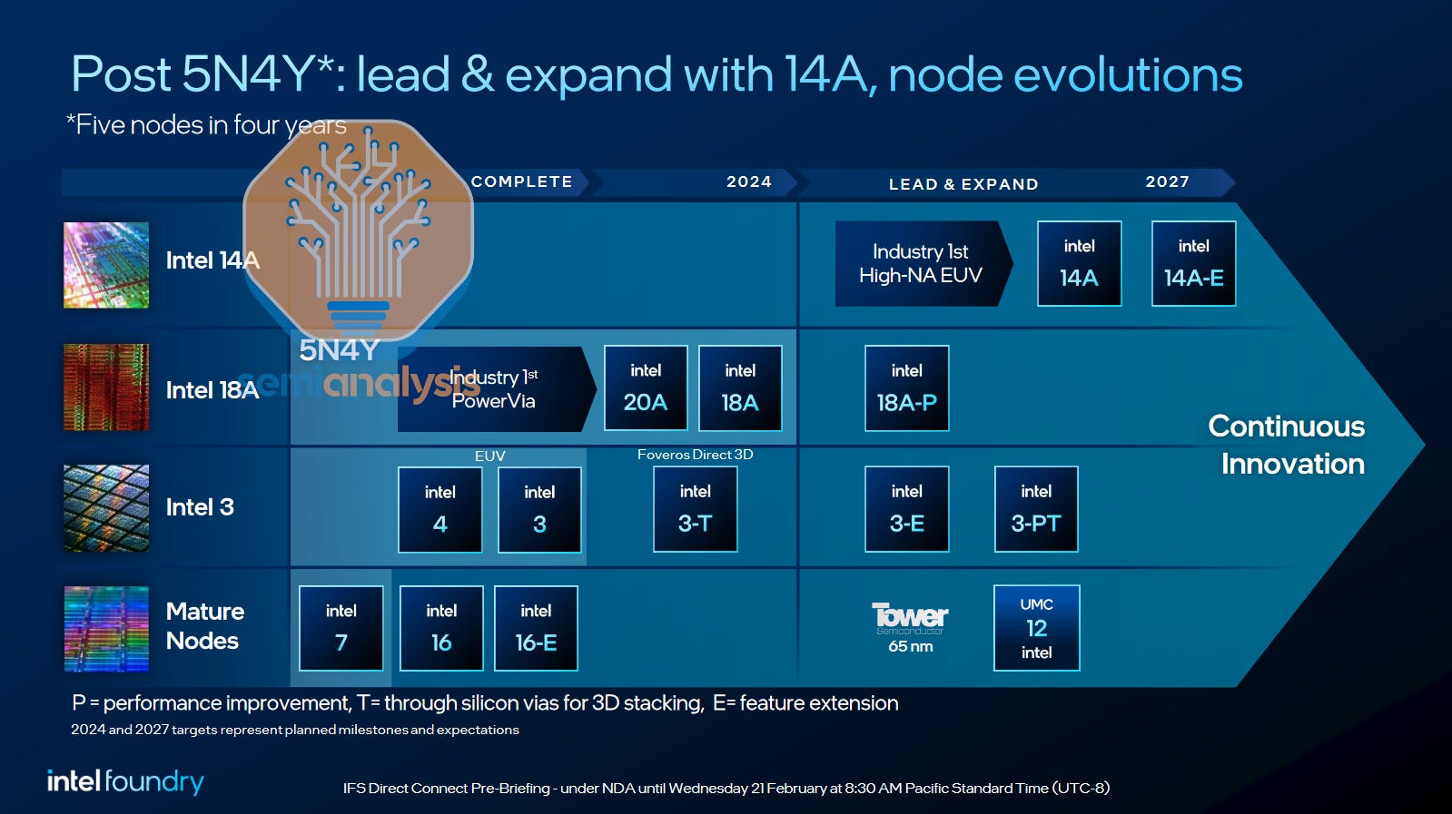
Now, it appears they are getting back on track. Intel’s Technology Development team (TD), led by Dr. Ann Kelleher, is trying to catch up. They are rapidly iterating on many node transitions trying to bring to market many new techniques from PowerVia, Backside Power Delivery, and new semi-damascene metallization schemes to new tooling such as Sculpta and High-NA EUV (even if it’s not cost effective). They have a variety of node variants coming with feature enhancements, performance increases, and even 3D TSV capabilities.

Intel claims that Intel 3 brings parity with performance per watt, but still leaves them behind the industry. They believe with 18A, they are ahead on performance per watt, and at parity elsewhere. At 14A in ~2027, Intel believes they will have an advantage on density and wafer costs as well. They believe it will even let them win mobile designs, not just high performance. We would push back somewhat on some of these claims based on N2 and N2P modeling.
These in research and development are amazing in their own right, but we have yet to see any real evidence of the last leg: high volume manufacturing. To be clear, they still do not have a single high-volume product on their Intel 4 or 3 process node. Intel claims that their Intel 4 process node has been “manufacturing ready” since December 6th 2022. It is now Q2 of 2024 and the only released product is Meteor Lake which has a compute tile that is ~70mm2. The Intel 4 component is smaller than most smartphone chips. Most the other tiles are from TSMC or on older nodes.
Furthermore, Meteor Lake has had paltry volumes due to its high-cost structure. We estimate COGS of more than 2x that of the Raptor Lake (Intel 7 monolithic) to fabricate. We estimate Meteor Lake has shipped in less than 10 million devices. That means even with poor yield assumptions, the total wafers run for Meteor Lake products in the market are less than 20,000 wafers for a whole year of production. For reference compare this to Apple’s monthly commercial shipping capacity of 45,000+ wafers on 5nm and 3nm today. Not as inspiring as Intel’s words.
Intel’s charts like the below from their foundry day also show that they have no plans of ramping Intel 4 production meaningfully. Intel 18A is only significant wafer volume in 2026.

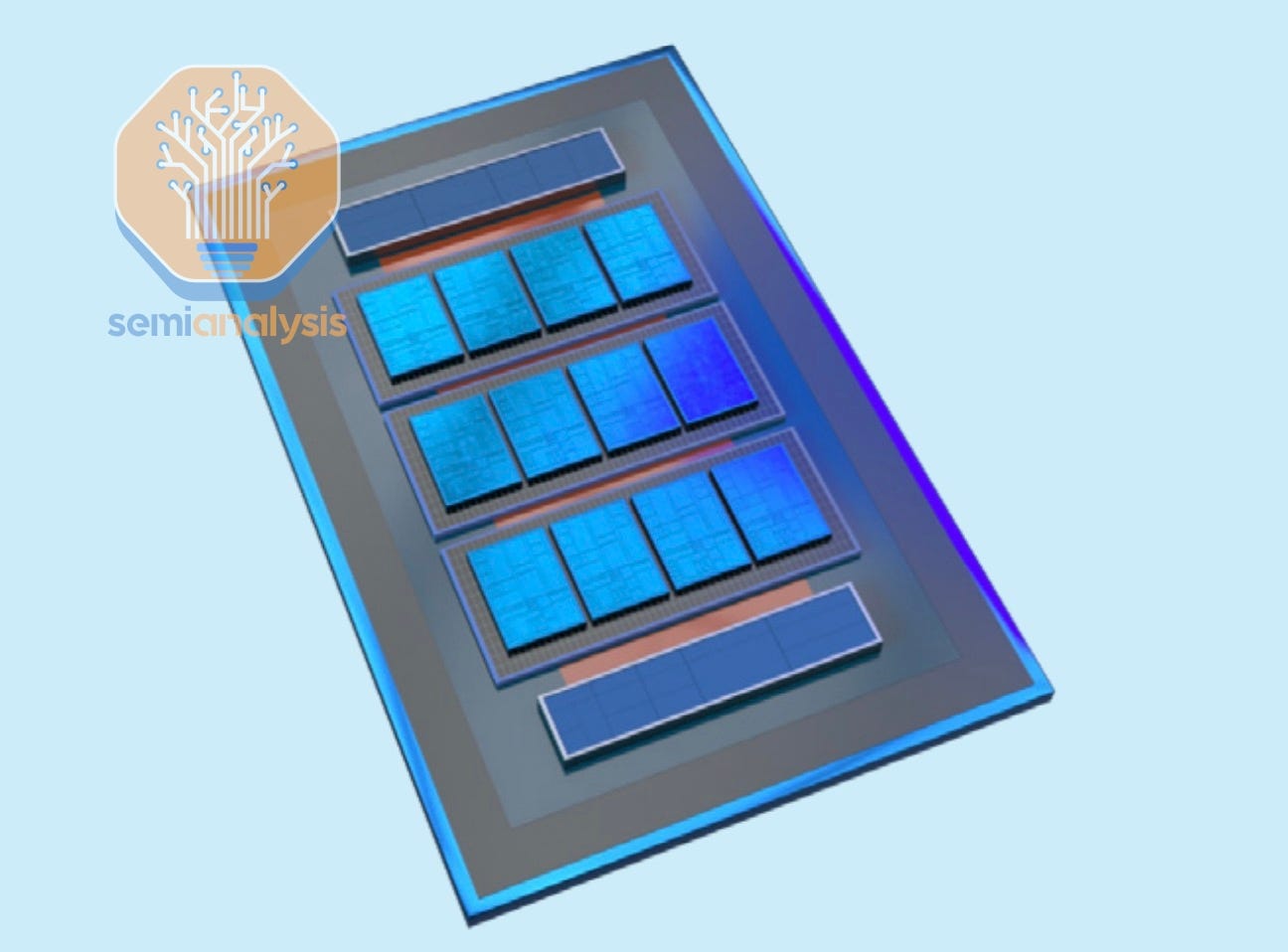
Despite this, there is still abundantly clear evidence showing that Intel is progressing rapidly. While Sierra Forest and Granite Rapids samples to major customers look decent, they are still not competitive with AMD’s Turin. Intel’s goal is to actually leapfrog Intel 4 and 3 in terms of volume production by the end of 2025 with 18A with new product launches that are actually competitive. Intel’s Clearwater Forest test chip has taped-out using 18A logic chiplets packaged on an Intel 3 base die with EMIB & Foveros Direct (Cu on Cu hybrid bonding – see our advanced packaging series for more details).
This is the first evidence of a crucial, if obvious, dynamic going forward: every leading edge fab must have a #1 customer driving it forward. That customer fills the leading edge fab. They justify further process development. Their chips prove out standard cells and intellectual property (IP) blocks on a new process, and they are reducing risk for the rest of the customer base. The takeaway here is simply that proving out building blocks on IP designs is necessary for Foundry to win outside customers.
That is perhaps the most exciting part about Intel’s foundry effort. They have got the leading EDA and IP companies, Arm, Synopsys, Cadence, Siemens (Mentor Graphics), and Ansys all investing heavily. There is a swath of IP coming from these vendors from Arm CPU cores, fabrics, die to die connectors, high speed 112G and 224G SerDes, PCIe 6 and 7, and various memory IP.
To be clear TSMC still has a tremendous advantage here, but Intel is focusing on closing the gap. An easy example is that TSMC had at least 7 companies tape out 224G SerDes on their 3nm, (Broadcom, Marvell, Nvidia, MediaTek, Alphawave, Synopsys, and Cadence), where as we are only aware of 1 for Intel’s 18A.
If this IP is delivered and it works well, then firms can actually come to Intel with their unique technology and package it with standard chiplets, IP, and existing and customizable Intel chips/datacenter/software platforms and come out with much more complete systems. At least that’s the pitch.

Publicly, Intel’s Product business units are free to choose whatever fab they see fit. While this is proven true in the short term – they are using TSMC N5 and N3 right now – it would be a death sentence for Foundry to lose that business long term. We’ve seen what happens: AMD leaving GlobalFoundries left the latter dead in the water for advanced node development. To win continuing Products business, Intel Foundries must continue driving its process technology – to the point of parity or better with TSMC, if indeed the Product side is free to choose any foundry. We think there is a bit of a finger on the scale for Product to use Foundry though, even if parity is all that is achieved.
The primary reason Intel needs foundry is volume. Costs of transistors continue to scale with shrinks. Intel admits in the 2nd half of the 2010s they had minimal cost scaling, but with the rapid progress to 7, 4/3, and 20/18A, they will bring back the economic scaling.
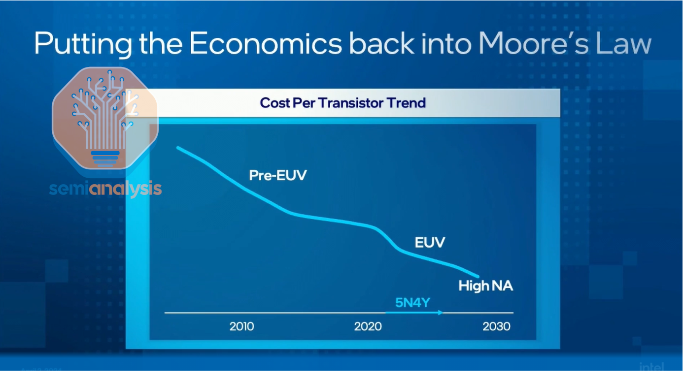
The misleading aspect of this chart is the volumes. Some folks claim transistor cost scaling stopped at 28nm, but that is wrong. The design costs incremented up massively with FinFET nodes. Fixed costs again increment up meaningfully with EUV, gate all around transistors, backside power delivery, and High-NA EUV.

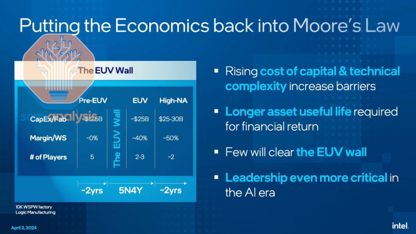
Intel says they needs $25B to $30B of capex per 10,000 wafers per week for their new fabs. TSMC has stated they requires about $42B of capex per 10,000 wafers for their 3nm in Arizona even after the “cost overruns”. We are unsure what the delta is for Intel versus TSMC on these numbers as the TSMC figures include site prep, shell, and tooling. Regardless, taking Intel’s numbers at face value, this is a huge wall given Intel always needs 150,000+ wafers per month of capacity on the leading edge to remain competitive in volumes with TSMC.
They do not have this today, but they need it or the business is unsustainable and dead. Today they cannot afford to build these fabs with their own cashflow. Let’s talk about how TSMC can do it sustainably and what Intel needs to do to replicate their success.
TSMC is enormously profitable and dominant, especially in leading edge logic. In pure foundry, Samsung has been a distant second place competitor (note that even Intel is discounting Samsung as a real player in logic foundry) and Intel is a work in progress in trying to get there. Despite this it is actually TSMC’s mature nodes that are more profitable on both an accounting profit and cash basis.
For semiconductor manufacturing, the biggest single cost is equipment. Wafer fabrication equipment is the majority of a fab’s capital expenditure with the remainder being capital spent on clean rooms. In the foundry company’s P&L, these capital costs are expensed as depreciation. From TSMC’s financials, depreciation expenses have historically been around 25-30% of revenue and usually more than 50% of TSMC’s COGS (most, but not all of that depreciation will flow through COGS).
Based on TSMC’s accounting policy, equipment is depreciated over a 5-year useful life. However, this does not reflect economic reality. Tools last a long time, the vast majority (>90%) of all semiconductor production tools that have been shipped since 1990 are still being used in the field today. Equipment that is older than 5 years will have almost zero depreciation cost associated with it (except for upgrades and servicing in some cases).
For TSMC’s nodes where most of the capacity is more than 5 years old, the big depreciation cost item won’t apply, making them very profitable in terms of gross margin. Furthermore, these nodes require little to no cash investments, which then fund expensive leading edge capacity expansions. The leading-edge capacity has lower margins and negative cashflow until multiple years after ramp.
As an IDM, Intel’s CPU-heavy product portfolio meant that their manufacturing focus was on leading edge processes. Intel didn’t maintain these “forever” nodes (although for a time it appeared as if Intel 14nm was going to be a forever node but not by choice) because their only customer (Intel themselves) had little need for them. Consequently, Intel didn’t have this ever-growing pool of mature wafer capacity that was capable of generating cash flow seemingly into perpetuity.


Instead, nodes would only be kept around for a few generations before being deprecated to make way for newer processes. While a lot of the equipment was reused and transitioned to newer technologies, they would also need to reinvest in new tooling for that transition. Now, as a foundry, Intel can sustain wafer demand for their nodes by filling capacity with external customers as internal demand goes down over time. This now supports their forever node strategy.
Building 150,000+ wafers a month of leading edge capacity requires a lot of investment – one key reason is that fabs must be built decked out with tools first before most customers will pay you for wafers (although there a few benevolent customers who are making small partial pre-payments). At Intel, this is all happening at a time when core business profitability is the weakest it has ever been, as Intel is getting crushed by competition. In 2023, Intel as a company was basically breakeven on operating profit compared to years of enjoying double digit operating margins.
This is even after Intel pulled out accounting tricks like extending equipment depreciation periods for equipment to 8 years from 5. Add on the additional ~$20bn of annual capital expenditure to ramp up all the new nodes and fabs and FCF has been negative over the previous 2 years. To plug the financing hole Intel has had to rely on a wide variety of capital sources to fund everything: traditional debt financing, government support, and even more creative financial engineering schemes like the Brookfield fab deal to find a way to pay for everything.

Other than the formidable government support, there are plenty of levers to pull, from simple measures such as utilizing additional headroom to raise more debt to more complicated co-investment deals with financial partners like the Brookfield Arizona Deal. Intel can not only look at co-investment for future fabs – perhaps in Ohio – but also can consider asset sale and leasebacks across their portfolio of fabs and other facilities. In the worst-case scenario, Intel can lean on the U.S. Government for further help as Intel’s capacity is vital to the goal of semiconductor onshoring.
While Intel has ~$120B of capital to tap, to get to our 150,000+ wafers a month sustainable target, they may need more than that. We are not sure where they can get this cash from. The process technology we believe is there. We aren’t sure who is willing to front the rest of these costs, as further financing would likely be a poison pill.
The biggest part of our net book value is obviously our PP and E [plant property and equipment] and most of that shows up in the foundry side. So I would say within a couple of years, that’s like $100,000,000,000 number net book value for just Intel foundry. And I think your knock on question here might be, well, how do you look at that in terms of valuation? And even the worst foundries are getting 2 times net book value and the best, of course, is getting 5 plus net book value. So this is where we think a lot of the value unlock in the business will come from is that net book value generating a good return.
Pat Gelsinger, Intel CEO
One interesting lever that Pat is already trying to pull is that bad foundries should be valued at 2x book valued. Perhaps this means Intel could tap capital markets to plug the capital gap.
The second half of this report will dive into Intel’s product group and segments. We will also discuss who we believe are the foundry business wafer and packaging wins and on what chips. We will also dive into AMD’s competitiveness.
