Hướng dẫn về BCD, CMOS, FinFET, SOI, GaN và SiC
Introduction to Semiconductor
Semiconductors have a small energy gap between the conduction and valance bands, and their conductivity is between insulators and conductors. At absolute zero temperature, semiconductor materials are pure insulators and gradually increase with temperature. Temperature and doping are the two mechanisms to manage the conductivity of semiconductors. Doping means the introduction of impurities into pure semiconductor elements such as Silicon, Germanium, Gallium, and Arsenide. Doping of pure semiconductor elements may produce an N-type or P-type crystal structure based on the doped element. Most semiconductor devices like diodes, transistors, and chips are made from various forms of P-type and N-type crystals junctions, as presented in Figure 1.

Figure 1 Typical model of PN-junction semiconductor
Importance of Semiconductor Technologies
In the digital industry semiconductors are the building block of every electronic device with a small size. The importance of semiconductor technologies nowadays is extended to everyday activities by facilitating connectivity and communications like smartphones. Semiconductors are an essential element in the electronics industry to perform complex tasks in a simplified and miniaturized manner. Semiconductor technologies are vital for the groundbreaking advancement of technological innovations and fast progress in many sectors like computing, communications, healthcare, and transportation. They easily support emerging technologies like AI, advanced imaging, and autonomous vehicles. Semiconductors provide good performance in terms of speed, and power efficiency reliability compared to older other technologies. In general, semiconductors are becoming a good enabler solution for most of the global challenges by utilizing them in innovative ways for multiple applications.
Overview of Different Semiconductor Technologies
This article will highlight types of semiconductor technologies including BCD, CMOS, FinFET, SiGe, FDSOI, SOI GaN, and SiC. The key features, applications, advantages, and disadvantages will be covered in comparative ways. A complementary Metal-Oxide Semiconductor (CMOS) is constructed by utilizing complementary pairs of N-type Metal-Oxide and P-type Metal-Oxide transistors. BCD technologies combine Bipolar Junction Transistors (BJT), CMOS, and Double Diffused Metal-Oxide Semiconductor (DMOS) on a single chip to enable high speed, low power, and high current handling operation of the chip. FinFET semiconductor technologies are the 3D structure of MOSFET around the silicon channel to improve the current flow control. SiGe (Silicon-Germanium) is a semiconductor technology that combines Germanium and silicon to enhance performance by boosting the mobility of electrons.
Moreover, many other semiconductor technologies are developing such as a fully Depleted Silicon-On-Insulator (FDSOI) to minimize the leakage currents and enhance performances and, a silicon-on-insulator (SOI) to minimize parasitic capacitances. Gallium Nitride(GaN) is a semiconductor technology with more advanced performance than silicon-based since it provides better electron mobility. Silicon Carbide(SiC) is a silicon and carbon-based semiconductor with a large voltage breakdown and good thermal freedom.
CMOS Technology
Basics of CMOS Technology
CMOS is a complementary-based semiconductor used in building integrated circuits (ICs). CMOS can be constructed from p-channel and N-channel MOSFET, complemented to create low-power logic gates and memory circuits. The invertor is a core of the CMOS and comprises nMOS and pMOS transistors to perform logic functions. As illustrated in Figure 2, pMOS transistors are connected to positive supply voltage and nMOSs to the ground. Almost no power without input change in CMOS as one side is always off.

Figure 2 Circuit diagram of CMOS
Its operations are simple and complementary; only one transistor is active at a time. When the input is high (logic 1), the pMOS is off, nMOS is on, and its output is low (logic 0). When the input is low pMOS is turned on, and nMOS is turned off, the output is high. CMOS components are self-isolation MOSFET transistors, which enable higher device density and integration of complex circuits on a small chip area.
Advantage and Disadvantage of CMOS Technology
As one of the semiconductor technology CMOS has many advantages and few dis advantages.
Advantages
Power consumption occurs only at switching events makes CMOS power efficient. CMOS is also highly versatile in producing logic gates, microprocessors, sensors, and memory and the interconnected feature enables massive transistors together to form a small-size IC. In addition, CMOS has a mature fabrication process making it cost-effective, suitable for mass production, and robust. CMOS has high noise immunity due to the MOSFET transistor’s self-isolation nature.
Disadvantages
Most of the disadvantages of CMOS are highly entangled with the fabrication process and packaging issues. They have high fabrication costs and complex design due to the cleanrooms require massive investment and fabrications cost. Susceptible to defects and leakage currents may be impacting during activities as its size is tiny. There is also a heating issue due to the massive number of transistors in a small area. They are highly affected by parasitic-like gate capacitances and resistance. The difficulty of scalability below 5nm is due to the quantum tunneling effect.
On the other hand, CMOSs are generally fast, however, they are not performing as fast as other technologies like BJT for high-speed applications. They are also easily affected by radiation and shortening channels. CMOS can handle digital tasks, nevertheless, they have a limited precision in analog performance compared to other technologies.
Application of CMOS Technology
As CMOS is a base for most of the ICs, its applications are summarized in the following table.
|
No. |
CMOS Applications |
Descriptions |
|
1 |
Logic circuits |
CMOS is a building blocks of AND, OR, NOT circuit
|
|
2 |
Microprocessors |
almost all modern CPUs used in computers, servers, smartphones, etc. are all built using CMOS process nodes |
|
3 |
RF and communication circuits |
CMOS used in RF applications for RF amplifiers, oscillators, and transceivers for wireless communication |
|
4 |
Memory Chips |
CMOS technology is the basics of many memories like SRAM and DRAM for high-density memory arrays. |
|
5 |
Mixed-signal ICs |
CMOS allows integration of analog and digital circuits on the same chip used in audio processing, data converters (ADC/DAC) |
|
6 |
Image sensors |
modern digital cameras use CMOS image sensors for better light sensitivity. |
|
7 |
Display drivers |
LCD and LED controllers use CMOS circuitry to deliver video signals |
|
8 |
Power management ICs |
due to the high efficiency of CMOS Battery chargers, voltage converters consume little power |
|
9 |
Consumer Electronics |
CMOS in a wide range of devices including televisions, game consoles, and home appliances. |
|
10 |
Medical devices |
Integrated circuits for imaging, diagnostics, and therapeutic equipment are designed in the CMOS process.
|
|
11 |
Automotive applications |
Automotive applications: various electronics systems based in CMOS in engine control units, and advanced driver assistance systems |
BCD Semiconductor Technology
Basics of BCD technology
BCD (bipolar-CMOS-DMOS) semiconductor is constructed by the integration of three types of transistor technology viz BJT, CMOS, and DMOS for the purpose of high-performance assimilation of analog and digital functions together in an efficient manner. DMOS is a modified MOSFET by a drain diffusion to enable higher voltage handling capability than conventional MOSFETs. Thus, BCDs can perform both logic levels due to CMOS and high voltage functions using BJT-DMOS. BCD is a complete system on chip with a mixed-signal design that improves the performance of older BiCMOS processors. In the manufacturing process, BCD contains a mounted silicon layer, followed by ion implantation for various transistor types. The metallic layers interconnect individual components, while isolation mechanisms are applied to prevent interferences among unalike transistors, as presented in Figure 3. BCDs are used in multiple microcontrollers, processors, and Mixed-signal ASICs as they enable the integration of cores, memory, I/O pins, ADC/DAC, and power transistors in small areas for complex embedded systems.

Figure 3 Schematic Diagram of BCD
Advantages and Disadvantages
Advantages
The BCD technology enables versatile design and a true system-on-chip IC with microcontrollers, memories, interfaces, and power circuits. The BJT component is very essential for high-speed signal processing and analog functions. CMOS is for minimal power digital functions. DMOS is applicable to high-power applications due to its voltage and current handling capability. BCD technology is less complex, has high-speed performance, and efficient power management.
Disadvantages
The integration of three technologies increases fabrication and design complexity. This leads to BCD’s high fabrication cost compared to CMOS. In addition, the complex layout creates unmanaged parasitic effects and difficulties in minimizing the defects across various device types.
Applications of BCD
The BCD semiconductor technologies are implemented as power management ICs to create smart power modules in voltage regulators, DC-DC converters, and battery system management. They drive various types of motors in the automotive and industrial sectors. Moreover, BCDs are core parts of microcontrollers that operate analog, digital, and power functions on a single chip. BCDs are utilized in multiple automotive, industrial, home appliance, medical, and telecom applications
FinFET Technology
Basics of FinFET Technology
FinFET is a type of non-planer of field effect transistor used in modern CPU and GPU fabrication processes adapted to overcome the difficulties related to conventional planer structures. The Fin refers to a thin strip of silicon extended on the top of the substrate, which acts as a conductive channel region. In a field effect transistor, the current flows through a channel when the applied voltage is at the gate. The wider contact area between the gate and the channel improves transistor efficiency. As shown in Figure 4, the contact area FinFET increases by a fin-shaped 3D structure. The 3D structure is better at reducing the short channel effect by better controlling electrostatics over the channel. Thus, the FinFET transistor improves its performance by reducing leakage current and minimizing parasitic capacitances as compared to the planner structure. Unlike a planner CMOS, a FinFET transistor is constructed on the three sides of a thin silicon.

Figure 4 Comparison of traditional planar structure to 3D FinFET semiconductor
Advantages and Disadvantages
The advantages and disadvantages of FinFET transistors are described below.
|
Advantages |
Disadvantages |
|
|
Reduce leakage current |
Complex 3D structure |
|
|
Improved gate control |
Higher manufacturing cost |
|
|
Better performance |
Contact resistance issues between source to drain |
|
|
High Current driving |
Increasing parasitic capacitances |
|
|
Greater Scalability |
|
|
Applications of FinFET
The FinFET process is used in advanced logic chip manufacturing below 10nm by major electronic companies such as Intel, Samsung, NVIDIA, and others for GUP and SoCs for high performance. The GPU from FinFET can be applicable to mobile devices, servers, computers, network equipment, AI accelerators, HPC systems, and wireless systems. FinFET transistors are used in widespread digital hardware due to the benefits of high-density and low-power consumption.
SiGe Technology
Basics of SiGe Technologies
SiGe is a type of semiconductor created by an alloy structure by adding a controllable Germanium(Ge) to Silicon (Si) to reduce the energy band gap of pure silicon for producing a hetero-structure bipolar transistor (HBTs) with emitter and base terminal different SiGe concentration, as illustrated in Figure 5. SiGe semiconductors perform better than traditional silicon bipolar transistors. In this technology, tuning the semiconductor energy band gap for specific applications is allowable by controlling the amount of Ge added to Si, which enables flexibility in controlling hole and electron mobility. The speed of the SiGe devices can be enhanced by adding more Ge composition but it is challenging for fabrication.

Figure 5 3D model of SiGe semiconductor
(Image credit: https://pubs.acs.org/doi/10.1021/acsaelm.2c00364)
Advantages and Disadvantages
Advantages
Compared to conventional Si-based bipolar transistors, SiGe technology improves current gain and maximum oscillation frequencies.
They also operate at high speed and low voltage with higher integration densities. The minority diffusion into the base terminal is also blocked by the heterojunction interface making them power efficient. SiGe semiconductor’s hole or electron mobility can be tuned by adjusting the amount of Ge on the Si element. SiGes have better compatibility with existing CMOS infrastructure and are more linear than other semiconductor technologies.
Disadvantages
Even though SiGe semiconductors have several advantages, they also increase fabrication complexity and cost, Nano-level scaling challenges and variations in SiGe mounting can impact the uniformity across devices. There is also a self-heating effect that constrained its power performance as well as parasitic effects due to additional junction degrading its performance when compared to homogenous transistors.
Applications of SiGe
SiGe transistors are more common in advanced communication and computing systems. Most RF circuits in cellular communication, high-speed wired networks, and near radio communications employ SiGe transistors. Especially, the emerging 5G, B5G, and 6G mm-wave and Terahertz communications, high-performance Mixed-signal ICs, and monolithic microwave integrated circuits(MMICs) are highly entangled with SiGe technologies. In addition, SiGe is used in ISM services and radar systems, fiber optic systems, automotive industries, and measurement devices.
FDSOI Technology
Basics of FDSOI
A Fully Depleted Silicon On Insulator (FDSOI) is a cutting-edge CMOS fabrication process employed for IC production, as shown in Figure 6. Unlike bulk silicon elements used in regular CMOS manufacturing, a thin layers of silicon is formed on a dielectric substrate to control electrostatics and minimize leakage current via the depleted transistor. When the transistors have zero leakage or power off, the ultra-thin silicon layer ensures full depletion of charge to enhance efficiency and performance compared to the bulk silicon one. The back-basing via the conducting substrate controls the threshold voltage and power characteristics.
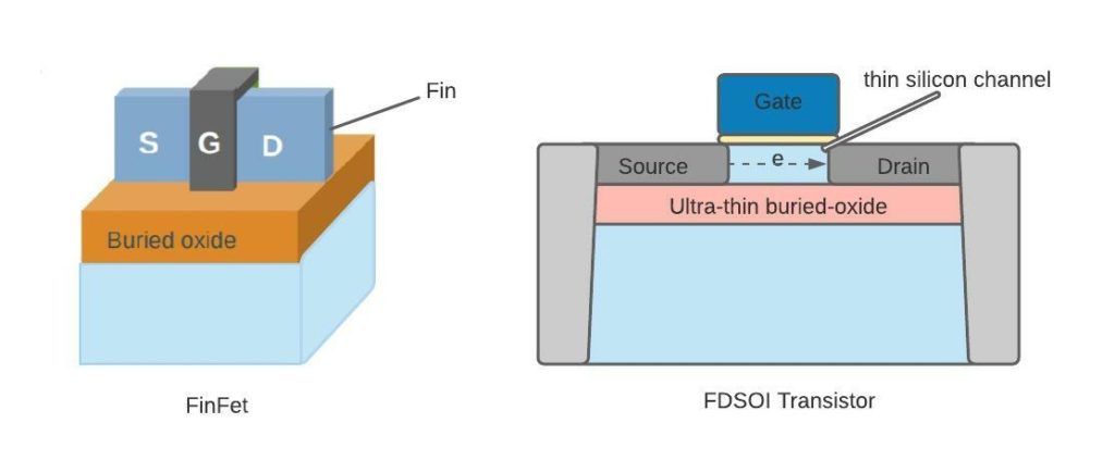
Figure 6 Fully depleted Silicon on insulator
Advantages and Disadvantages
Advantages
FDSOI transistors have better short-channel performance and operate at low voltage compared to traditional bulk silicon technology, which means a significant reduction of dynamic and static power utilization. They are compatible with existing CMOS infrastructure and minimize variability compared to traditional bulk silicon devices and FinFET transistors. A number of transistors are compiled in a small-size chip in FDSOI technology. They are also more flexible in threshold voltage tuning through the back bias.
Disadvantages
FDSOI transistor production has additional costs in producing a silicon-on-insulator and transferring a thin film on the substrate. Due to this, there is a non-zero capacitance between device layers and dielectric material. Moreover, they have a low drive current, limited scaling due to thickness versus electrostatics, and high sensitivity to defects.
Application of FDSOI
FDSOIs are used in many mission-critical applications like aerospace electronics. They are applicable in multiple devices like smartphones and tablets with efficient power utilization. They are also implemented in the Internet of Things, automotive industries, computing, and networking equipment for energy efficiency and to minimize space constraints. Moreover, FDSOIs are preferred in medical electronics for implantable devices and factory automation equipment since they are highly energy-efficient and durable.
SOI Technology
Basics of SOI
SOI semiconductor refers to a layered silicon-insulator-silicon substrate microchip instead of conventional silicon chips, as shown in Figure 7. That means a thin layer of silicon is located on electrically insulated silicon oxide and attached to a silicon base substrate to get some performance improvement by reducing parasitic capacitance. The modern SOI process implements a separation by implantation of oxygen (SIMOX) technology for bonding, unlike buried silicon on an insulator in the earlier process. SOI transistors are either partially depleted (P-SOI) or fully depleted (FDSOI) depending on the film thickness, which affects the performance and efficiency of the SOI with smaller sizes.

Figure 7 Architecture of SOI semiconductor
Advantages and Disadvantages
Advantages
The insulated material improves electrical isolation between adjacent devices to minimize power loss and assist in high-speed operation at RF computation. SOI transistors have lower junction capacitors and leakage current improves its performance and reduces noise. The insulation also reduces alpha particles which is a cause for soft errors in memory cells. They are highly compatible with CMOS and easily fabricated compared to FinFET transistors.
Disadvantages
Most of the disadvantages of SOI semiconductors are related to insulating materials. It must have a high dielectric constant to control the electrostatic with a thin silicon body. The wafer bonding method also adds cost and manufacturing complexity to chip production. SOI chips still have non-zero parasitic capacitances between the insulating material and the silicon and the device is characterized by the thickness and uniformity over the entire chip.
Applications of SOI
SOI semiconductors are more common in many electronic components, microprocessors, and embedded systems where high speed and low power operation is highly demanded. Thus, they are used in mobile devices and wireless infrastructure for their power efficiency, networking equipment, and industrial automation due to their reliable operation, and high-speed computing devices.
GaN (Gallium Nitride) Technology
GaN is a semiconductor technology that consists of gallium and nitrogen, as presented in Figure 8. This compound has a better bandgap (typically 3.4 ev) than other semiconductor technologies. GaN conducts electricity at high voltage and high frequency. GaN has higher breakdown voltage, better electron mobility, and good thermal conductivity than silicon semiconductors.

Figure 8 GaN semiconductor technology
(Image credit: https://www.isit.fraunhofer.de/en/technology/power-electronic/semiconductor-technology-for-powerdevices/gan.html)
Advantages and disadvantages of GaN
Advantages
GaN semiconductor highly reduces the size and weight of power systems while improving their efficiency. It can also have extended and advanced with different technologies like High Electron Mobility Transistor (HEMT) with GaN-on Si for low cost and GaN-on SiC high thermal conductivity, they provide more extended performance than GaN itself. GaN HEMTs operate at 600+ voltages and switch fast with low loss.
Disadvantages
GaNs require expensive and limited substrate material. Their fabrication faces several challenges while growing high-quality semiconductors. Its fabrication requires 2D electron gas at the interface between Gallium and Nitrogen, thus increasing manufacturing costs and difficulties.
Applications of GaN
GaN is commonly used in power-switching applications like battery charging, LED lighting, data center power supply, electric vehicle (EV) electronics, and high-frequency switching. In addition, GaN is implemented in energy infrastructure, lighting, industrial instrumentation, and consumer electronics utilize GaN.
Silicon Carbide (SiC) Technology
Basics of SiC
SiC technology is another wide bandgap (typically in 2.9-3.3 eV ranges) semiconductor that comprises Silicon and Carbon, as shown in Figure 9. The wider bandgap permits it to operate at higher temperatures, voltages, and frequencies compared to silicon semiconductors. The most common SiC semiconductor types are 4H-SiC and 6H-SiC, which are fabricated similar to MOSFET or JFET,

Figure 9 Silicon carbide (SiC) semiconductor
Advantages and Disadvantages of SiC
Advantages
SiC transistors can operate at higher temperatures and have high breakdown voltage. They have better thermal properties and can quickly dissipate heat energy, which allows a compact design without a heat sink. SiC transistors also reduce conduction loss and switching losses. SiC transistors have a ten times higher critical electric field and three times wider bandgap and thermal conductivity than silicon-only transistors.
Disadvantages
SiC fabrication is a little costly compared to Si-only transistors since it is challenging to integrate small substrates in a controlled doping mechanism and native oxide formation for MOSFETs. SiC substrates are limited in availability, so mass production is difficult. The existence of high leakage current and compatibility with existing CMOS infrastructure are also other disadvantages of SiC.
Applications
Due to their operated voltage range and efficiency, SiCs are commonly used in power electronics. Many inverters, converters, chargers for electric vehicle systems, industrial motor drives, and power supplies use SiC transistors. Power factor correction circuits and renewable energy systems use SiC as a switch. In UPS to enhance charging and discharging batteries, aviation power systems, substations, and gas industries for telemetry, industrial heating, and power distributions. Thus, SiCs are used for high-power, high-temperature applications where efficiency, reliability, and compact size are critical.
Future Trends
In future semiconductors, several emerging and novel technologies are being researched. Heterogeneous integration with silicon into Group-III and Group-V elements leads to a high mobility of electrons for enhanced RF, sensing, and optical applications. In addition, other novel transistors with atomically thin body effects from Graphene and black phosphorus are under investigation. For controlling better electrostatics at nano-scale and non-planner structures like FinFET and mitigate devices are explored. Researchers are expecting other options as a paradigm.

Conclusion
In semiconductor technology, silicon is the most commonly used element due to its availability and matured manufacturing process. However, its operation is limited in temperature, power efficiency, and breakdown voltage. By minimizing limitations to improve performances, several techniques have been employed in the semiconductor industry like silicon-on-insulator (SiO), FDSOI, CMOS, FinFET, SiGe, SiC, and GaN for efficient power utilization, high-speed performance, high frequency, and high voltage operation. Each technology has its specific advantages and disadvantages when designed for particular applications. Almost all advancements require additional manufacturing costs.