Hướng dẫn thiết kế PCB cứng nhắc
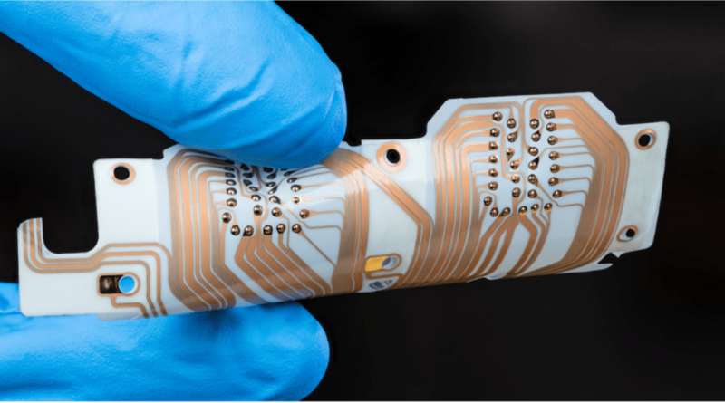
In today’s electronics industry, compact, efficient, and versatile PCBs are in high demand. Rigid-flex technology allows engineers to design boards that bend and flex without compromising performance or reliability.

Mastering rigid-flex PCB design can be challenging due to its unique requirements. Whether you’re an experienced designer expanding your skills or new to the field, this article introduces a simplified, structured approach to rigid-flex PCB design.
The article emphasizes adhering to flex-specific rules and using tools like ODB++ for effective communication with fabricators about multi-zone stackup details. Whether working on flex-only or flex-rigid designs, these principles offer a universal foundation for creating robust, innovative rigid-flex PCBs.
How Flex Differs from Rigid PCB Design
There are only a few differences between executing rigid and flex PCB designs in a PCB design tool.
Regional Stackups
- Each board region can have a unique stackup.
- Regions are defined by separate board outlines, each labeled as either “rigid” or “flex.”
- Board outlines must share at least one side.
- A master stackup, combining all regional stackups, drives the tool.
Flex-Specific Layer Types
- Special layers like flex core, cover layer, adhesive, and stiffeners are supported.
Names Solder Mask Layers
- Separate mask layers can be added for each board region, beyond the traditional top and bottom solder masks.
Flex Elements in the Pad Stack
- The pad stack includes cover layer openings for through hole and SMD pads, and pads defining hole openings in stiffeners.
Bend Areas
- Bend areas define where and how the flex circuit bends, used in DRC and 3D design.
Fabrication Output
- Design intent and regional stackups are conveyed to the board fabricator via Xpedition Layout ODB++ output, the preferred format for flex and flex/rigid designs.
A simple 10-point rigid-flex design process
- Set the “rigid-flex”-technology before starting your design. This notifies layout that you are doing a flex/rigid-flex design.
- Create a master stackup that has all layers from all regions of the board included.
- Define multiple board outlines. Give each a name to identify each sub- board and give each a type: flex or rigid. Even if a single flex outline is used, the name and flex technology must be set.
- Assign subsets of layers from the master stackup to each outline, thus defining the stackup for each region.
- Establish route borders. If multiple board out- lines have been created, the appropriate route borders must be created per board outline.
- Create bend areas. Attributes on each bend area defines the bend radius, bend angle and direction of bend as well as a few settings controlling if vias and components are allowed in the bend zone.
- Place and route as usual. All outer layers can be used for placement and components will automatically end up on the correct layer when placed. Thus, the same component can be placed in any of the board outlines without cell or pad stack alterations.
- Display in 3D if desired. 3D can show flat or folded assembly and use the bend areas to model the fold.
- Run appropriate DRC checks. Several flex specific rules are checked in real time with “correct by design” and some rules are checked in batch DRC.
- Create outputs. All output engines can export manufacturing data for a flex or flex/rigid design. ODB++ is especially well suited and can correctly convey the multi-zone stackup to the fabricator.
At this point, we have the fabrication data for our rigid-flex design, concluding our step-by-step guide. This 10-point design process serves as a structured roadmap, guiding you through each phase of rigid-flex PCB development.
Whether working with flex-only designs or complex flex-rigid configurations, the principles here will equip you with the knowledge and skills needed to navigate the challenges of rigid-flex PCB design confidently.

For a more detailed explanation of this rigid-flex design flow, please download the full whitepaper, Rigid-Flex PCB Design Guidelines. It includes a primer on how to create stackups, define board outlines, layer assignment, route borders, and more, with clear instructions and illustrations. Key aspects like bend areas, place and route procedures, 3D visualization, design rule checking (DRC), and manufacturing outputs are also given deeper treatment.
Remember, mastering rigid-flex design is a continuous learning process. As you apply these principles, you’ll encounter unique scenarios and opportunities for innovation. Embrace these challenges, seek continual learning, and use the insights from this guide to push the boundaries of rigid-flex PCB design.
Gregory Beers
Gregory Beers has been helping Siemens Digital Industries Software customers with all things printed circuit board and flex/rigid-flex related for more than 13 years. He has over 30 years of experience as an electrical engineer, 25 of those years specializing in military communications and guidance systems. In addition, Beers had owned and operated a service bureau for complete product engineering services for 25 years before coming to Siemens.


