Google Launches Its Second OpenMPW Free Silicon Chip Program, on GlobalFoundries' 180nm Node – Hackster.io
Please ensure that JavaScript is enabled in your browser to view this page.
Google has announced the opening of its Open Multi Project Wafer (OpenMPW) program for GlobalFoundries' 180nm process node, allowing free and open source silicon projects to send their creations off for production into silicon chips absolutely free of charge.
"Following the announcement about GlobalFoundries joining Google's open source silicon initiative, we are now sponsoring a series of no-cost OpenMPW shuttle runs for the GF180MCU PDK [Process Design Kit] in the coming months," explain Google's Ethan Mahintorabi, Johan Euphrosine, and Aaron Cunningham in a joint announcement. "Those shuttles will leverage the existing OpenMPW shuttle infrastructure based on the OpenLane automated design flow with the same Caravel harness and the Efabless platform for project submissions."
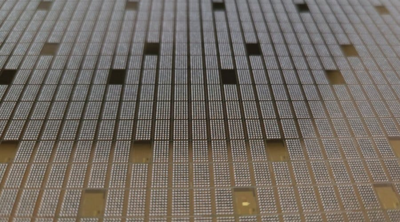
The OpenMPW program launched as a partnership between silicon fab SkyWater, design platform Efabless, and Google back in 2020, providing a means for free and open source silicon projects to have their designs created as physical chips at zero cost. Designs are built using the open process design kits provided by the fabs on a standardised "shuttle," and fabricated on a multi-project wafer before being sliced and packaged.
Google announced the GlobalFoundries open PDK release, which is based on the company's 180nm process node, in August this year, describing it as a "milestone […] in the foundry ecosystem market." Like the SkyWater 130nm and later 90nm PDKs, the GlobalFoundries PDK allows anyone to design for production on the company's 180nm process node license-free — and now, with the launch of the latest OpenMPW shuttle program, cost-free too.
As with the earlier SkyWater shuttles, the production runs will be limited to 40 projects — each of which must make its design available under an open source license, be reproducible using nothing but the sources and the GlobalFoundries PDK, and have to pass pre-manufacturing checks. A short-run "test shuttle" will iron out the kinks, followed by additional shuttle runs with what Google promises will be "a longer project application window and improved testing."
Those interested in submitting a design for production under the program can create a new project on Google's open silicon landing page, and have until December 5th, 2022 to get their submission in for inclusion on the first shuttle.
Hackster.io, an Avnet Community © 2024
