Động lực của Analog Bits và hướng tới tương lai

Analog Bits is aggressively moving to advanced nodes. On SemiWiki, Dan Nenni covered new IP in 3nm at DAC here. I covered the new Analog Bits 3nm IP presented at the TSMC Technology Symposium here. And now, there’s buzz about 2nm IP to be announced at the upcoming TSMC OIP event in September. I was able to get a briefing from the master of analog IP, enology and viticulture Mahesh Tirupattur recently. The momentum is quite exciting, and I will cover that in this post. There is another aspect to the story – the future impact of all this innovation. Mahesh touched on some of that, and I will add my interpretation of what’s next. Let’s examine Analog Bits momentum and a look to the future.
The Momentum Builds
The Analog Bits catalog continues to grow, with a wide array of data communication, power management, sensing and clocking technology. Here is a partial list of IP that is targeted at TSMC N2:
Glitch Detector (current IP): Instant voltage excursion reporting with high bandwidth and voltage fluctuation detection. Delivers circuit protection and enhances system security in non-intended operation modes. IP can be cascaded to function similar to a flash ADC.
Synchronous Glitch Catcher (new IP): Multi-output synchronized glitch detection. Reports voltage excursions above and below threshold during the clock period with high bandwidth. Improved detection accuracy with system clock alignment that also facilitates debugging and analysis.
Droop Detector (enhanced IP): Extended voltage range 0.495 – 1.05V with higher maximum bandwidth of 500MHz. Differential sensing and synchronous voltage level reporting. Precision in monitoring with continuous observation and adaptive power adjustment. A pinless version that operates at the core voltage is in development.
On-Die Low Dropout (LDO) Regulator (enhanced IP): Improved power efficiency. Fast transient response and efficient regulation and voltage scalability. Offers integration, space savings, and noise reduction. Use cases include high-performance CPU cores and high lane count, high-performance SerDes.
Chip-to-Chip (C2C) IO’s (enhanced IP): Supports core voltage signaling. Best suited for CoWoS with 2GHz+ speed of operation and 10GHz+ in low-loss media.
High-Accuracy PVT Sensor (enhanced IP): Untrimmed temperature accuracy was originally +/- 8 degrees C. An improved version has been developed that delivers +/- 3.5 degrees C. Working silicon is available in TSMC N5A, N4 & N3P. The figure below summarizes performance.

Looking ahead, accuracy of +/- 1 degree C is possible with trimming. The challenge is, the trimming is affected by the die temperature, making it difficult to achieve this accuracy. Analog Bits has developed a way around this issue and will be delivering high accuracy PVT sensors for any die temperature.
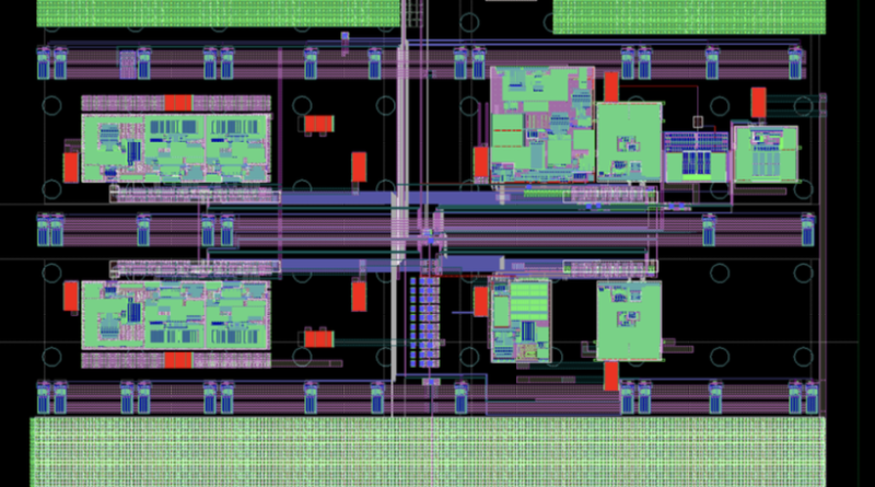
This background sets the stage for what’s to come at the TSMC OIP event. In September, Analog Bits will tape out a test chip in TSMC N2. Here is a summary of what’s on that chip:
- Die Size: 1.43×1.43mm
- Wide-range PLL
- 18-40MHz Xtal OSC
- HS Differential Output Driver and Clock Receiver – Power Supply Droop Detector
- High Accuracy PVT Sensors
- Pinless High Accuracy PVT Sensor
- LCPLL
- Metal Stack – 1P 15M
The graphic at the top of this post is a picture of this test chip layout. In Q1, 2025 there will be another 2nm test chip with all the same IP and:
- LDO
- C2C & LC PLL’s
- High Accuracy Sensor
The momentum and excitement will build.
A Look to the Future
Let’s re-cap some of the headaches analog designer face today. A big one is optimization of performance and power in an on-chip environment that is constantly changing, is prone to on-chip variation and is faced with all kinds of power-induced glitches. As everyone moves toward multi-die design, these problems are compounded across lots of chiplets that now also need a high-bandwidth, space-efficient, and power-efficient way to communicate.
If we take an inventory of the innovations being delivered by Analog Bits, we see on-chip technology that addresses all of these challenges head-on. Just review the list above and you will see a catalog of capabilities that sense, control and optimize pretty much all of it.
So, the question becomes, what’s next? Mahesh stated that he views the mission of Analog Bits is to make life easier for the system designer. The solutions that are available and those in the pipeline certainly do that. But what else can be achieved? What if all the information being sensed, managed and optimized by the Analog Bits IP could be processed by on-chip software?
And what if that software could deliver adaptive control based on AI technology? This sounds like a new killer app to me. One that can create self-optimizing designs that will take performance and power to the next level. I discussed these thoughts with Mahesh. He just smiled and said the future will be exciting.
I personally can’t wait to see what’s next. And that’s my take on Analog Bits momentum and a look to the future.
Share this post via:


