Diamond Breakthroughs Shape Future of High-Performance Electronics
//php echo do_shortcode(‘[responsivevoice_button voice=”US English Male” buttontext=”Listen to Post”]’) ?>
Diamond, renowned for its exceptional properties, has long held promise for various applications, yet its potential as a semiconductor has faced hurdles hindering commercialization. Recent strides made by Advent Diamond have tackled critical technical challenges—notably, by fabricating single-crystal diamond doped with phosphorus to create n-type layers.
This advance is pivotal because phosphorus represents diamond’s sole relatively shallow n-type dopant. The successful incorporation of phosphorus into diamond enables the realization of electronic devices that harness diamond’s unparalleled attributes. This includes its exceptional thermal conductivity, wide bandgap and robust mechanical properties. By surmounting previous limitations, this breakthrough unlocks a new era for diamond-based technologies, promising advancements in fields like quantum sensing and computing, high-power electronics and radiation detection.
In an interview with EE Times, Advent Diamond co-founder and CEO Manpuneet Benipal discussed the pivotal role of her company and expertise in diamonds in advancing various technological fields. “My Ph.D. research in materials science and engineering, particularly focused on semiconductors and materials used in semiconductor devices, laid the foundation for my work in diamond technology,” she said.

Benipal’s experience includes developing the initial fabrication processes for diamond PIN emission diodes during her tenure at Arizona State University (ASU). Later, as a senior research engineer at ASM America, she honed her skills in material processes crucial for semiconductor devices.

By MRPeasy 05.01.2024


By Global Unichip Corp. 04.18.2024
“At Advent Diamond, I initiated the development of diamond semiconductor devices from the ground up, recognizing the unique challenges and opportunities presented by diamond as a wide-bandgap material,” she said.
Her work at Advent involves identifying and testing crucial aspects of diamond semiconductor devices, including diamond device architecture, metallization, passivation and developing lab-to-fab–ready fabrication processes.
Benipal noted the importance of understanding the interplay between material defects, subsurface polishing damage and overall material quality in optimizing diamond device performance.
“We collaborated closely with ASU to pioneer doped and intrinsic diamond material layers, overcoming critical material challenges detrimental to device performance,” she said.
Through these efforts, Benipal and her team at Advent Diamond made significant strides in advancing the capabilities of diamond-based semiconductor technologies, paving the way for transformative applications in various industries.
Diamond features
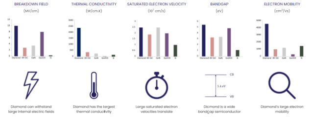
Diamond has substantial benefits over typical semiconductor materials like silicon and silicon carbide, especially in applications that need great performance and durability. Its extraordinary thermal conductivity, which exceeds that of conventional semiconductors, tackles significant thermal management difficulties, a major barrier for semiconductor devices that operate at high power densities. Furthermore, diamond’s high carrier mobility and saturation velocity allow for better performance in terms of frequency operation and power management than traditional materials.
Diamond’s unique characteristics are generating significant R&D efforts in the semiconductor sector. As demand increases for sophisticated semiconductor components with improved performance and downsizing, diamond appears as a possible next-generation wide-bandgap material. This has piqued the curiosity of defense contractors and commercial organizations intent on researching diamond’s potential and using it for diverse technologies to overcome present semiconductor limits.
“Diamond’s unmatched thermal conductivity and carrier mobility pave the way for groundbreaking advancements in high-frequency semiconductor devices,” Benipal said. This underscores the transformative impact that diamond-based technologies could have across telecommunication, electrification and quantum applications. The pursuit of diamond semiconductor solutions represents a strategic shift toward addressing the longstanding challenges with traditional semiconductor materials, unlocking new opportunities for innovation and application development in diverse industries.


Technology
One of Advent Diamond’s core innovations is the ability to grow single-crystal phosphorous-doped diamond on preferred substrates, and it is the only U.S. entity with this capability. Phosphorous doping is particularly significant, as it enables the creation of n-type semiconductors in diamond, a crucial element for electronic device development. Additionally, Advent Diamond has achieved milestones in growing boron-doped diamond layers on large areas, expanding the potential applications for diamond-based electronics.
Intrinsic diamond layers with extremely low impurity concentrations have been developed using sophisticated growth techniques protected by trade secrets, ensuring the highest quality and performance standards for semiconducting-grade diamond materials. Advent Diamond’s expertise extends beyond material growth to encompass comprehensive component design, fabrication and characterization capabilities. This includes advanced cleanroom processes, such as etching, lithography and metallization, alongside a suite of characterization techniques like microscopy, ellipsometry and electrical measurements.
The innovative diamond-based radiation detectors that Advent Diamond is developing offer a transformative solution for defense, commercial and scientific markets. By leveraging doped and intrinsic semiconducting diamond layers, these detectors are superior in detecting energetic particle radiation with exceptional radiation hardness and noise-suppression capabilities. The versatility of these detectors spans applications ranging from ultraviolet light and alpha particles to X-rays and protons, underscoring the breadth of Advent Diamond’s technological reach.
“Advent Diamond is leading the development of matured doped [p-type and n-type] and intrinsic diamond material layers, along with components/devices crafted from these superior-quality diamond layers for applications in electrification, telecommunications and quantum technologies,” Benipal said. “Diamond exhibits remarkable electrical and material properties, surpassing those of GaN and SiC, and our goal is to translate these properties into exceptional semiconductor device performance. Our vision is to introduce diamond semiconductor devices boasting unparalleled specifications and performance to the commercial market, spurring innovation in electrification, telecommunications and quantum applications. We place particular emphasis on surface treatments, such as reactive ion etching and diamond-compatible chemical mechanical polishing, to reduce defects, enhance interfaces, improve uniformity and crystallinity, and maintain controlled doping concentrations throughout various thicknesses of doped and intrinsic diamond layers. This approach ensures the creation of superior-performance diamond semiconductor devices, radiation sensors and quantum materials/devices for widespread commercial adoption. Advent Diamond is poised to be the first to market with diamond RF diodes and other groundbreaking semiconductor devices.”

Challenges of diamond-based semiconductor devices
Diamond-based semiconductor devices are experiencing a surge in interest and investment across industries like aerospace, healthcare and renewable energy. Researchers and private entities are focused on advancing diamond technology to address specific challenges in high-power and high-frequency applications.
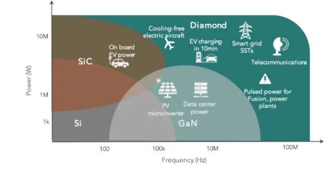
“Diamond promises to meet these needs and bring innovation with enhanced performance,” Benipal said. “For applications like faster EV charging stations, solid-state transformers, electrification of aircraft and telecommunications, there is increasing demand for semiconductor devices, which can operate at higher power and higher frequency.”
Currently, diamond semiconductor development focuses on research and scalability. Companies, organizations and government agencies are working together to address issues like diamond wafer size, defect density and material improvements critical to realizing its promise. Moreover, diamond wafers have significant fault density, limiting device performance and dependability. The majority of accessible wafers have fault levels that exceed the threshold necessary for optimal semiconductor functioning.
According to Benipal, mosaic diamond wafers of 1 to 2 inches are available, with efforts underway to increase wafer sizes to 4 inches. However, defect densities remain a critical issue, with most wafers exhibiting about 108 defects/cm2 or higher. There is a need to improve diamond wafer quality and reduce defect densities to unlock their full potential.
“It is important to bring defects down to 103 defects/cm2 to achieve expected performance,” Benipal said.
To address these challenges, DARPA and other agencies are funding scalable diamond technology projects, emphasizing the development of high-quality materials and advanced semiconductor devices. Globally, research groups are focused on improving diamond device structures like diodes, transistors and integrated circuits. This collaborative effort aims to propel diamond-based semiconductors into mainstream applications, enhancing performance and reliability in critical sectors.
Future and manufacturing process
The landscape of diamond semiconductor devices is undergoing a transformative shift propelled by emerging manufacturing techniques and advancements in diamond synthesis. Techniques like plasma-enhanced chemical vapor deposition and refined diamond growth processes are paving the way for enhanced diamond-based electronics. According to industry experts, these advancements are crucial for driving innovation and addressing evolving needs across various sectors.
“Diamond has physical properties like no other semiconductor, which makes it the most promising material to eliminate challenges that exist because of current materials’ physical limits,” Benipal said.
One major factor driving this progress is precise control over doping during diamond deposition. Doping during growth procedures enables uniform and regulated concentration, which is crucial for improving semiconductor performance. According to Benipal, unlike ion implantation, which has limitations owing to diamond’s hardness, chemical vapor deposition appears as a scalable and desirable approach for generating doped and inherent diamond materials. This scalable deposition technology has the potential for commercialization, boosting efforts in diamond wafer fabrication and semiconductor development.
The journey toward high-performing diamond semiconductor devices encounters hurdles like structural damage caused by ion bombardment, which can deteriorate material quality. However, ongoing innovations in diamond polishing methods, such as chemical polishing and refined surface-smoothening techniques, mitigate these challenges. These advancements aim to prepare epi-ready diamond surfaces with minimal defects and superior material quality.
“Developments in diamond materials and the potential for stabilized quantum states with intentional doping will be revolutionary for quantum applications,” Benipal said.
Looking ahead, diamond-based electronics hold immense potential in meeting the demands of electrification and telecommunications. The unique physical properties of diamond, coupled with ongoing development efforts, offer a pathway to overcome current material limitations. Moreover, in the quantum computing sphere, diamond’s ability to provide stable quantum states for qubits through controlled doping promises groundbreaking advancements.
Advent Diamond is innovating RF receiver protector diodes with >1-kA/cm2 current densities, ideal for radar systems. Diamond’s exceptional properties allow for high-power and -frequency performance, surpassing conventional diodes. It boasts unrivaled thermal conductivity, acting as a self-cooling heatsink, and excels at elevated temperatures up to 400°C, reducing thermal runaway risk.
“Our roadmap includes all diamond high-power diodes and transistors [EV chargers, solid-state transformers], space-qualified components and high-quality PQuantum Diamond [a new material] for stable quantum properties and quantum components,” Benipal said.
According to Benipal, the future of diamond-based electronics hinges on refining manufacturing processes, enhancing material quality and leveraging diamond’s exceptional properties to pioneer innovative solutions across diverse sectors, from high-frequency telecommunications to quantum applications.


