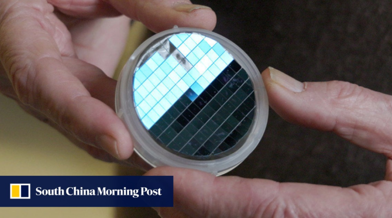
Chinese-US team creates first graphene semiconductor in likely computing leap – South China Morning Post
Graphene is a simple material, made up of just a single layer of carbon atoms, said to be a million times thinner than human hair. But it is stronger than almost anything else in nature, and beats silicon hands down when it comes to electronic potential.
Ever since graphene was discovered in 2004, scientists have tried to use it, in combination with other carbon materials, to devise a new kind of chip – one that would use less power and work faster than any semiconductor in existence.
This long-elusive feat might now be close to reality, according to nano scientists at China’s Tianjin University and the Georgia Institute of Technology, whose findings were published in the journal Nature on Wednesday.
Chinese state media hailed the feat as a momentous step forward for the use of graphene in chip manufacturing.
“This research has not only maintained graphene’s remarkable stability but also introduced fresh electronic traits, clearing the path for graphene-based chips,” Beijing-based Science and Technology Daily said in a report on Friday.
The study was led by professors Ma Lei from Tianjin University and Walt de Heer from Georgia Tech. Both have focused on graphene electronics and other two-dimensional materials since they set up the Tianjin International Centre for Nanoparticles and Nanosystems at Tianjin University in 2018.
Known as the first stable two-dimensional material at room temperature, graphene’s distinctive electronic structure also means it has zero “bandgap” – meaning there is no energy difference when electrons in semiconductors jump between low and high energy bands. The lack of this natural gap hinders graphene’s semiconductor capabilities, making it less suitable for electronic devices.
Overcoming this challenge without losing graphene’s intrinsic properties is a key step towards its practical use in electronics, Ma told China Business Network.
“The reason our research is valued is that it can truly make graphene electronics practical in the future and remove the biggest obstacle.”
The new method creates a special layer on graphene that generates the needed gap for electrons and allows them to move very quickly, much faster than in silicon and similar materials.
This is a big step forward for using graphene in electronic devices, giving it the right properties to function well as a semiconductor.
To achieve this breakthrough, Ma and his team used a method called quasi-equilibrium annealing, which involves carefully heating and cooling a material to modify its structure.
The process begins with heating a silicon carbide substrate in a furnace and then maintaining it at various temperatures for specific durations. This results in the formation of smooth, flat surfaces, ideal for adding a layer known as “epigraphene”.
The layer is crucial as it introduces a necessary electron gap, making graphene suitable for electronic devices.
It also ensures that the graphene is durable and easy to work with, holding out promise for its widespread commercial application in electronic devices.
“It not only opens new paths for high-performance electronic devices beyond traditional silicon-based technology but also injects new energy into the semiconductor industry,” a report on the Tianjin University website said.
“The emergence of graphene semiconductors is timely, heralding a fundamental transformation in electronics. This innovation fulfils the growing demand for higher computing speeds and miniaturised integrated electronic devices.”
As for the practical application of graphene semiconductors, Ma said the material could be cost-competitive in comparison with semiconductor materials currently in the market, while offering superior performance.
However, the journey is likely to be a long one. Ma estimated that it might take another 10 to 15 years to fully realise the industrial implementation of graphene semiconductors.


