Cải thiện điện dung ký sinh trong các thiết bị DRAM thế hệ tiếp theo
As conventional DRAM devices continue to shrink, increases in parasitic capacitance at smaller dimensions can negatively impact device performance. New DRAM structures may be needed in the future, to lower total capacitance and achieve acceptable device performance. In this study, we compare the parasitic capacitance of a 6F2 honeycomb dynamic random-access memory (DRAM) device to the parasitic capacitance of a 4F2 vertical-channel-access-transistor (VCAT) DRAM structure. The results indicate that the 4F2 structure significantly reduces parasitic capacitance between the node contacts (NC) and the bitlines (BL) compared to the 6F2 structure. Although parasitic capacitance between other components of the 4F2 device increase slightly compared to the 6F2 device, they remain at acceptable levels to support target device performance. The total parasitic capacitance for the 4F2 DRAM device is effectively reduced compared to the 6F2 device, which may provide superior performance at smaller device dimensions.
Introduction
As conventional 6F2 DRAM devices continue to shrink, parasitic capacitance increases between the bitline and the Node Contact (CBL-NC) due to a smaller distance between these DRAM components. This increase in capacitance causes the bitline sensing margin and refresh times to degrade, negatively impacting memory performance. To address this issue and significantly reduce parasitic capacitance, a 4F2 VCAT DRAM architecture is proposed for next-generation DRAM devices.
Traditionally, Si wafer-based experimentation has been used to evaluate new DRAM architectures, but this can be time-consuming and costly. In this study, we use virtual process modeling with SEMulator3D, instead of wafer-based experimentation, to evaluate parasitic capacitance between the 6F2 and 4F2 DRAM devices.[1] We review various parasitic capacitance sources present in different DRAM structures and evaluate potential improvements in total capacitance that might be achieved in 4F2 DRAM devices compared to 6F2 DRAM devices.
Device structure and simulation methods
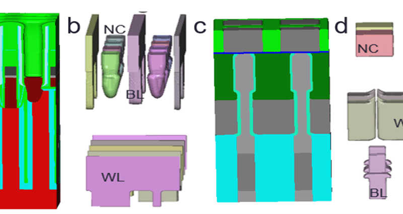
In this study, virtual 3D structures were constructed in the process modeling platform using a combination of layout data and process step data. Figure 1a shows a simulated 3D structure of a 6F2 DRAM device, along with its net component structure (figure 1b). A simulated 3D structure of a 4F2 DRAM device and its net component structure are shown in figures 1c and 1d, respectively. Capacitance extraction was performed on these structures to calculate parasitic capacitance in each of the DRAM devices.
Fig. 1: 6F2 DRAM simulation (a) 3D structure, (b) net component structure; 4F2 DRAM simulation (c) 3D structure, (d) net component structure.
Device simulation results
Figure 2 displays the parasitic capacitance simulation results for the 6F2 and 4F2 DRAM devices. CBL-NC is significantly reduced in the 4F2 DRAM structure, mainly due to the large spacing between the BL and NC compared to the 6F2 DRAM. CBL-WL and CWL-NC are larger in the 4F2 DRAM primarily because the wordline is not buried and it is closer to the bitline than in a 6 F2 DRAM. CBL-BL is comparable because there is not much difference in the BL structure between 4F2 and 6F2 DRAM devices. CWL-WL and CNC-NC are worse in 4F2 DRAM due to their larger CD and smaller spacing compared to the values found in 6F2 DRAM. Overall, the total parasitic capacitance is still significantly reduced in a 4F2 structure compared to a 6F2 structure.
Fig. 2: 6F2 and 4F2 DRAM device parasitic capacitance simulation result.
4F2 DRAM device performance is improved in comparison with the 6F2 DRAM device. CBL-NC is effectively reduced in the 4F2 structure compared to the 4F2 structure, along with the total capacitance (see figure 2). Some subcomponents of parasitic capacitance increase using the 4F2 structure, but these capacitance values are far lower than the CBL-NC found in the 6F2 structure, leading to lower total capacitance. This means there is a sufficient process window to achieve an acceptable device performance. CWL-WL remains the largest parasitic capacitance component in a 4F2 DRAM, after the large reductions in CBL-NC. compared to a 6F2 DRAM. Unfortunately, wordline-to-wordline capacitance will affect control of the transistor gate, so additional attention may need to be paid to device control in a 4F2 DRAM design.
Conclusion
Virtual process modeling was used to study the capacitance for different DRAM structures. Our results indicate that total parasitic capacitance can be significantly reduced in a 4F2 DRAM structure compared to a 6F2 DRAM structure, due to a reduction in the dominant parasitic capacitance (CBL-NC) present in 6F2 DRAM devices. 4F2 DRAM structures may offer improved performance to 6F2 devices, particularly as device dimensions decrease.
References
- Q. Wang, Y. De Chen, J. Huang, B. Vincent and J. Ervin. 2022 China Semiconductor Technology International Conference (CSTIC)2022, pp. 1-4.
Dempsey Deng
Dempsey Deng is a semiconductor and process integration engineer at Coventor, a Lam Research Company. Deng previously worked at United Microelectronics Corporation (UMC) in ReRAM process development. Prior to his work at UMC, Deng worked at both Xiamen Silan Jike Microelectronics and Changjiang Storage Technology as an etch process engineer, where he was responsible for 32/64P channel hole etch process development and optimization of back-end metal CT processing. Deng holds a MS degree in Materials Science from the Wuhan Institute of Technology.


