Cách giải quyết hiện tượng nhiễu tần số trong POL đúng thời gian liên tục bằng mạch tiêm gợn sóng
The purpose of this article is to walk through the steps of implementing a ripple injection circuit for constant on-time POLs. It covers how to connect the circuit and then how to calculate the values used in the circuit.
Frequency jitter can be caused by a number of things such as noise injection into the voltage sense lines from outside sources, to very low ripple current in the output inductor reducing the amount of needed ripple fed back into the feedback of the voltage regulator (VR) necessary to provide optimal performance and regulation. We will not get into the theory of constant on-time control in this article. It is important to know that the ripple injection circuit described below injects this needed ripple into the feedback of the VR for optimal performance if needed.
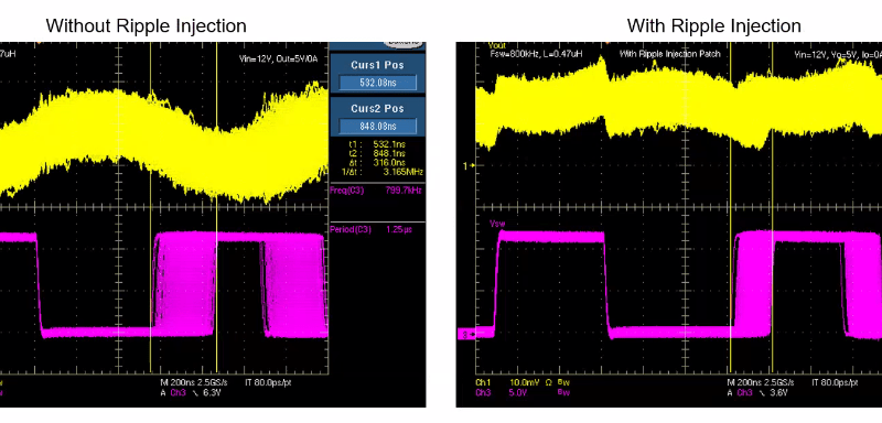
Frequency jitter may not be an issue if it is minimal and does not cause too much ripple on the output of the VR. The frequency jitter is measured at the switch node. See the example below. The waveform on the left shows ~316 ns of jitter on the switch node (purple waveform) which impacts the output voltage ripple (yellow waveform). With the ripple injection circuit added in the waveform on the right the jitter is reduced to ~200ns and the output voltage ripple peak-peak reduces.
The ripple injection circuit is very small, consisting of 2 small capacitors (C1 & C2) and 1 small resistor (R1), and is added to the VR circuit as shown below. It is important to connect C1 between RFB1 and the bode resistor, if the circuit has a bode resistor, to ensure it does not impact the bode measurement. If there is no bode resistor, which is okay, connect C1 and RFB1 directly to Vout.
Calculating the values for the ripple injection circuit is not difficult and can be done in Excel. First, it is important to know Vref for the POL. In analog POLs, Vref is equal to the feedback voltage and can be found in the datasheet. In digital POLs, Vref can be determined by first knowing what Vout scale loop (VSL) is set to. VSL will be 1:1 for lower voltage output rails, or 1:2 for higher output voltage rails. An example of Vout settings based on VSL is shown below.
Finally, to calculate R1, C1, and C2, refer to the below formulas.
For digital POLs: Vref = Vout for VSL = 1:1, and Vref = Vout/2 for VSL = 1:2.
For analog POLs: Vref = Vfb and can be found in the datasheet.
Determine Co (output capacitance) using the de-rated capacitance instead of the nominal capacitance.
R1 can be adjusted to improve phase margin or jitter. A smaller R1 value reduces the bandwidth of the VR, which slows down the transient response.


