Bộ nhớ băng thông cao (HBM): Hướng dẫn cơ bản
HBM presents a significant leap over traditional memory types. Key features such as astonishing memory bandwidth, reduced power consumption, impressive memory capacity, and swift transfer rates distinguish HBM from its predecessors. Understanding these characteristics is essential for appreciating the impact of this cutting-edge technology.
Embark on a journey through the intricacies of High Bandwidth Memory with this ultimate guide. Discover the evolution of HBM, its vital applications across various industries, the advantages it offers over conventional DRAM, and the future of memory configurations in the computing world. Welcome to the gateway of knowledge on High Bandwidth Memory.
High Bandwidth Memory Market Size was valued at USD 2.8 Billion in 2022. The high bandwidth memory market industry is projected to grow from USD 3.53 Billion in 2023 to USD 22.573 Billion by 2032, exhibiting a compound annual growth rate (CAGR) of 26.10% during the forecast period (2024 – 2032).
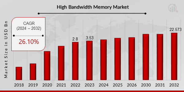
Image source: Market Research Future
Key Features of High Bandwidth Memory
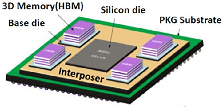
High Bandwidth Memory (HBM) has been revolutionizing the way high-performance computing systems manage data flow. One of its most notable features is the considerable increase in bandwidth compared to traditional memory solutions. HBM achieves this through the use of stacked DRAM chips interconnected by through-silicon vias (TSVs) and microbumps. This innovative design allows for much shorter data paths, resulting in improved data speed and electrical efficiency.

Image source: Micron
The integration of multiple memory chips into a single package not only enhances the power efficiency but also reduces the memory’s footprint on the PCB. By leveraging a wide-interface architecture, HBM facilitates increased transfer rates and lower power consumption. Unlike conventional memory systems that struggle to balance performance with power budget, HBM offers a memory solution tailored for the power efficiency and performance demands of high-performance computing, graphics cards, and machine learning applications.
Memory Bandwidth
At the heart of High Bandwidth Memory’s prowess is its stellar memory bandwidth. Bandwidth memory, in HBM’s case, refers to the capacity to move large amounts of data quickly between the memory and the processor. HBM utilizes a wider memory bus and operates across independent channels allowing simultaneous data access, significantly expanding the amount of data transferred per cycle. Such an enhancement can immensely benefit applications that require high-speed data processing, like advanced graphics rendering or complex scientific calculations.
Power Consumption
The efficient architecture of HBM has enabled it to stand out in terms of power consumption. Unlike conventional DRAMs, which require higher power to drive signals over long distances, HBM’s vertically stacked ICs and shorter connection paths notably reduce the energy required per bit transferred. This translates to better power efficiency, essential for keeping the power budget in check, especially in dense electronic packages often found in high-performance computing environments and advanced nodes in semiconductor engineering.
Memory Capacity
With a focus on vertical stacking and the use of silicon interposers, HBM can achieve greater memory capacity within a single package compared to traditional flat memory solutions. By stacking multiple DRAM chips on top of one another, HBM not only conserves space but also provides considerable scope for scaling memory capacity as needed without the typical area constraints faced by PCB designers. This aspect of HBM makes it an appealing memory device for systems that require a large memory capacity within a constrained power and space envelope.
Transfer Rates
High Bandwidth Memory boasts impressive transfer rates, a critical consideration for systems that rely on the swift movement of data. The design of HBM allows for wide interface buses, leading to transfer rates that can significantly surpass those of conventional memory types. With HBM’s transfer rates, systems benefit from faster load times, smoother data processing, and an overall boost in performance, making it suitable for tasks that involve high data throughput, such as video processing and neural network training.
The Evolution of High Bandwidth Memory Technology
The trajectory of memory technology has been a relentless pursuit of balance between multiple facets: capacity, speed, power efficiency, and size. At each juncture of this journey, innovations have addressed the limitations of previous generations. This evolution has led to the emergence of High Bandwidth Memory (HBM), a game-changing leap forward that has reshaped the performance landscape of memory solutions.
Traditional Memory Solutions
In the realm of traditional memory solutions, systems typically relied on Double Data Rate (DDR) SDRAM, with its subsequent iterations (DDR2, DDR3, DDR4) offering incremental advancements in performance and power efficiency. However, these conventional memories operated with a parallel bus interface, which faced challenges like signal integrity and routing congestion as the demand for bandwidth and capacity increased. Additionally, broader memory buses required more physical space and power to operate, which in turn affected system design and thermal management.
Introduction of High Bandwidth Memory
The introduction of High Bandwidth Memory represented a significant paradigm shift. HBM redefined data transfer by implementing a stacked memory architecture, with multiple DRAM chips piled high, interconnected by through-silicon vias (TSVs) for ultra-fast signal transmission. This 3D packaging technique significantly widened the data interface without increasing the footprint, allowing for high-speed communication directly adjacent to the processing unit. With this innovation, HBM dispelled the limitations that plagued traditional flat memory designs, offering substantially more bandwidth and diminishing the power-consumption curve.
Advancements in High Bandwidth Memory Technology
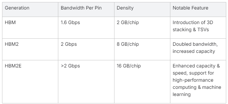
As HBM technology progressed, each iteration brought about formidable advancements. HBM2, for example, doubled the bandwidth per pin and improved density over its predecessor. Following that, HBM2E extended capacity and speed even further. These advancements have made HBN crucial for the latest graphic-intensive tasks and burgeoning fields such as artificial intelligence and machine learning, which demand rapid and vast memory capabilities. Seamlessly integrating into the silicon interposer, HBM operates alongside advanced nodes in semiconductor engineering to catalyze computational might while adhering to stringent power budgets in condensed electronic real estate.
The table below summarizes the evolutionary milestones of HBM:
With relentless advancements, HBM continues to propel the technological envelope, enabling unprecedented performance for next-generation computing applications.
Applications of High Bandwidth Memory
High Bandwidth Memory (HBM) has emerged as a transformative memory solution, finding applications in a spectrum of areas where speed, efficiency, and capacity intersect at critical junctures. Its ability to handle large volumes of data at impressive speeds while being power-efficient makes it an ideal choice for various computing paradigms. We’ll explore its vital role in high-performance computing, graphics, artificial intelligence, and datacenter applications, illustrating how its unique attributes meet the ever-increasing demands for rapid data processing and transfer.
High-Performance Computing
High-Performance Computing (HPC) encompasses a broad range of systems that deliver vastly superior computational power, enabling complex tasks like scientific simulations, climate modeling, and advanced materials research. HPC systems require memory that can keep pace with their formidable processing capabilities, and HBM fulfills this need exquisitely.
- Performance-Driven: HBM’s stacked configuration provides multiple channels working in parallel to maximize data throughput.
- Power-Efficient: Despite its high-speed data transfer rates, HBM maintains a lower power consumption profile, which is critically important in HPC environments where power usage is a key operational concern.
- Density: With improved density per chip, HBM allows HPC systems to manage more extensive data sets without compromising on physical space.
Graphics Applications
The correlation between HBM and graphics applications is particularly strong, as the need for memory bandwidth intensifies with advancing graphic resolutions and complexities.
- High Resolution and Frame Rates: Graphics Processing Units (GPUs) with HBM can render high-resolution images and videos at elevated frame rates, necessary for modern gaming, virtual reality, and professional visualization.
- Smooth Performance: The high bandwidth enables steady data flow, allowing for smooth performance even under intense graphical loads.
- Compact Form-Factor: HBM’s small footprint allows for compact and efficient graphics card designs, an important feature for sleek consumer electronic devices.
Artificial Intelligence
Artificial intelligence (AI) and machine learning (ML) models often require immense memory bandwidth to efficiently train on large datasets. HBM provides the capability needed to support the intensive workloads of AI applications.
- Fast Data Access: Quick access to memory is crucial for the iterative processes of AI and ML algorithms, and HBM delivers on this with its superior transfer rates.
- Parallel Processing Support: HBM facilitates the parallel processing capabilities required for complex AI computations.
- Efficient Scaling: As AI models grow in size and complexity, HBM’s scalability ensures memory isn’t a bottleneck for development.
Datacenter Applications
Datacenters are the backbone of the digital economy, supporting cloud computing, content delivery, and enterprise services. HBM can play an integral role in optimizing datacenter operations.
- Bandwidth for Virtualization: Datacenters benefit from the increased bandwidth when running multiple virtual machines or containers, as it allows for more data to be processed concurrently without delays.
- Energy Savings: HBM’s power efficiency translates to significant cost savings for datacenters, where power consumption is a significant operational expense.
- Low Latency: The low-latency characteristics of HBM improve response times, contributing to faster service delivery and improved user experience.
In conclusion, the extensive applications of High Bandwidth Memory underscore its importance as a core technology driving the future of complex computational tasks. With each generation of HBM, the potential applications expand, promising to sustain the insatiable demand for faster, more efficient, and denser memory solutions.
Advantages of High Bandwidth Memory
High Bandwidth Memory (HBM) has secured its place as a significant innovation in memory technology, primarily due to its distinct advantages over conventional DRAM solutions. By resolving some of the critical limitations faced by traditional memory, such as bottlenecks in data transfer rates and energy inefficiency, HBM has become a cornerstone for applications demanding high-speed data processing and minimal latency. Let’s delve into the specific advantages that set HBM apart, highlighting increased memory bandwidth, improved power efficiency, high memory capacity, and faster transfer rates.
Increased Memory Bandwidth
The defining feature of High Bandwidth Memory is its expansive memory bandwidth capabilities. Unlike traditional memory devices that may struggle under heavy workloads, HBM employs a wide interface constructed through stacking multiple DRAM chips and using silicon vias for interconnection. This method enables a much larger number of independent channels to operate simultaneously, drastically increasing the total available memory bandwidth. In practical terms, this translates into the swift handling of large volumes of data, a crucial factor in many contemporary applications, from high-performance computing to the latest graphics cards.
High Memory Capacity
Besides bandwidth and power efficiency, HBM also boasts a high memory capacity housed within a compact physical form factor. The vertical stacking of DRAM chips with HBM results in a memory solution that offers greater density and, thereby, a larger capacity in a single package. Such a configuration is amenable to systems with limited space yet requires substantial memory, such as compact, high-performance GPUs found in workstation laptops and small form-factor devices.
Faster Transfer Rates
Finally, HBM provides blistering transfer rates – a direct result of its architectural design. With multiple memory banks functioning in unison across a broad interface furnished with high-speed silicon vias, data transfer occurs at a rate substantially quicker than what’s achievable by conventional memory solutions. This improved transfer performance ensures that data-intensive operations, particularly in areas like machine learning, where speed is a make-or-break factor, are not throttled by memory latency.
In summation, High Bandwidth Memory represents a breakthrough type of memory that addresses key challenges faced by various types of memories. Its architecture is carefully tailored to provide a high-performance memory solution that dovetails with the contemporary demands of advanced computing. As a consequence of these intrinsic advantages, HBM stands out as an essential ingredient for emerging technologies and high-end computing platforms seeking to make the leap into the future.
High Bandwidth Memory Configurations
High Bandwidth Memory (HBM) is renowned for its high-speed, high-capacity, and energy-efficient design that caters to the demands of modern high-performance computing environments. The unique configurations of HBM enable it to deliver multiple times the bandwidth of traditional memories. The ingenuity behind HBM lies in its innovative layouts, which come in various configurations to maximize performance and minimize space usage. These HBM configurations include 3D-stacked memory designs and the advanced 5D multi-die package systems. The configuration choice often balances the demands for bandwidth, power consumption, and physical space within devices such as graphics cards and machine learning accelerators.
5D Multi-Die Package Systems
5D multi-die package systems are the zenith of packaging technology, aiming for unparalleled performance. As an evolution of 3D stacking, these systems add an extra dimension of integration, combining multiple layers of 3D stacked chips to form an immensely powerful and efficient memory solution. The “5D” refers to three spatial dimensions plus two additional dimensions of integration, including the interconnects and package-level assembly. This method meticulously coordinates each die’s operation, enabling even faster transfer rates and lower power consumption, all while maintaining a small footprint on the hardware board.
3D-Stacked Synchronous Dynamic Random-Access Memory (3D-Stacked DRAM)
When it comes to HBM, 3D-stacked DRAM stands as a key technology. It involves stacking multiple layers of dynamic RAM (DRAM) dies on top of each other, connected via Through-Silicon Vias (TSVs). These TSVs run through the silicon wafers, enabling a vertical electrical connection between different layers of the stack. This 3D stacking not only saves space but also contributes to lightning-quick data transfer rates and enhanced bandwidth, influential for real-time data processing in high-performance computing scenarios.
3D-Stacked Memory Architectures
The 3D-stacked memory architectures represent a leap in memory design, combining several layers of integrated circuits (ICs) into a single package. By stacking memory dies, HBM effectively minimizes the signal distance and presents vast improvements in latency and energy efficiency compared to 2D configurations. These architectures employ micro-bumps and TSVs for dense inter-die connectivity, which in turn streamlines the communication pathways between memory cells. This condensed arrangement significantly bolsters the available bandwidth per chip, making HBM an optimal memory solution for bandwidth-intensive applications.
3D Configurations and Stacking Techniques
Delving into the specifics of 3D configurations, there are various stacking techniques employed to realize HBMs. Techniques like die-to-die bonding and the use of a silicon interposer are commonplace. A silicon interposer, placed between the memory dies and the substrate, provides a large routing area for TSVs, ultimately allowing for a more robust and dense package. As for the die-to-die bonding approach, it employs direct copper connections between dies, eschewing the need for an interposer. These stacking methods contribute to the efficiencies of signal transmission, power distribution, and heat dissipation in HBMs, thus optimizing their overall functionality within a memory ecosystem.
High Bandwidth Memory vs. Traditional DRAM Solutions
High Bandwidth Memory (HBM) has emerged as a frontrunner in the realm of memory technologies, especially when compared to traditional DRAM solutions. This form of memory technology is designed keeping in mind the intense requirements of contemporary high-performance computing, graphics rendering, and advanced machine learning algorithms, which demand not just higher speeds but also greater bandwidth and energy efficiency. HBM achieves these goals through innovative design configurations such as 3D stacking and advanced packaging techniques, differentiating it from the conventional flat, planar layouts of traditional DRAM.
Memory Bandwidth Comparison
One of the most prominent advantages of HBM over traditional DRAM is the substantial bandwidth it provides. HBM features wide-interface memory buses and multiple independent channels working in parallel, vastly enhancing the data transfer capacity. To illustrate, a typical HBM configuration could offer a bandwidth of around 256 GB/s or more, which is several times the bandwidth provided by traditional DRAM that might hover around 32 GB/s. This stark difference allows for much faster data processing, proving essential in bandwidth-hungry scenarios.
Power Usage Comparison
Power efficiency is yet another area where HBM shines in comparison to traditional DRAM. The layered design of HBM means that data travels shorter distances, and the memory operates at lower voltages, reducing the overall power consumption. While traditional DRAM’s power usage can be a limiting factor especially in power-sensitive applications, HBM’s architecture is tailored to maintain high performance on a lesser power budget. The precise power savings can vary, but HBM often demonstrates a significant reduction in power consumption per gigabyte when compared to its traditional counterparts.
Memory Capacity Comparison
When it comes to memory capacity, traditional DRAM modules have long been relied upon to provide substantial storage. However, HBM introduces a paradigm shift with its stacking capabilities, permitting the vertical integration of dies and enabling significantly denser memory configurations within the same or even smaller footprint. As a result, HBM can achieve greater density, and thus higher memory capacity within a single stack, without the need to increase the physical size of the memory device.
Transfer Rates Comparison
Transfer rates, or the speed at which data is read from or written to the memory, are critical for overall system performance. HBM offers exceptional transfer rates owing to short data paths in its 3D stacked architecture and high-speed Through-Silicon Vias (TSVs). Compared to traditional DRAM, which may reach transfer rates of about 8 to 14 Gbps, HBM can boast rates well above 100 Gbps. This allows much more efficient handling of data-intensive tasks, propelling advancements in computer graphics, scientific computing, and real-time analytics.