Bao bì nâng cao TSMC khắc phục sự phức tạp của thiết kế nhiều khuôn
The TSMC Technology Symposium provides a worldwide stage for TSMC to showcase its advanced technology impact and the extensive ecosystem that is part of the company’s vast reach. These events occur around the world and the schedule is winding down. TSMC covers many topics at its Technology Symposium, including industry-leading HPC, smartphone, IoT, and automotive platform solutions, 5nm, 4nm, 3nm, 2nm processes, ultra-low power, RF, embedded memory, power management, sensor technologies, and AI enablement. Capacity expansion and green manufacturing achievements were also discussed, along with TSMC’s Open Innovation Platform® ecosystem. These represent significant achievements for sure. For this post, I’d like to focus on another set of significant achievements in advanced packaging. This work has substantial implications for the future of the semiconductor industry. Let’s examine how TSMC advanced packaging overcomes the complexities of multi-die design.
Why Advanced Packaging is Important
Advanced packaging is a relatively new addition to the pure-play foundry model. It wasn’t all that long ago that packaging was a not-so-glamorous finishing requirement for a chip design that was outsourced to third parties. The design work was done by package engineers who got the final design thrown over the wall to fit into one of the standard package configurations. Today, package engineers are the rock stars of the design team. These folks are involved at the very beginning of the design and apply exotic materials and analysis tools to the project. The project isn’t real until the package engineer signs off that the design can indeed be assembled.
With this part of the design process becoming so critically important (and difficult) it’s no surprise that TSMC and other foundries stepped up to the challenge and made it part of the overall set of services provided. The driver for all this change can be traced back to three words: exponential complexity increase. For many years, exponential complexity increase was delivered by Moore’s Law in the form of larger and larger monolithic chips. Today, it takes more effort and cost to get to the next process node and when you finally get there the improvement isn’t as dramatic as it once was. On top of that, the size of new designs is so huge that it can’t fit on a single chip.
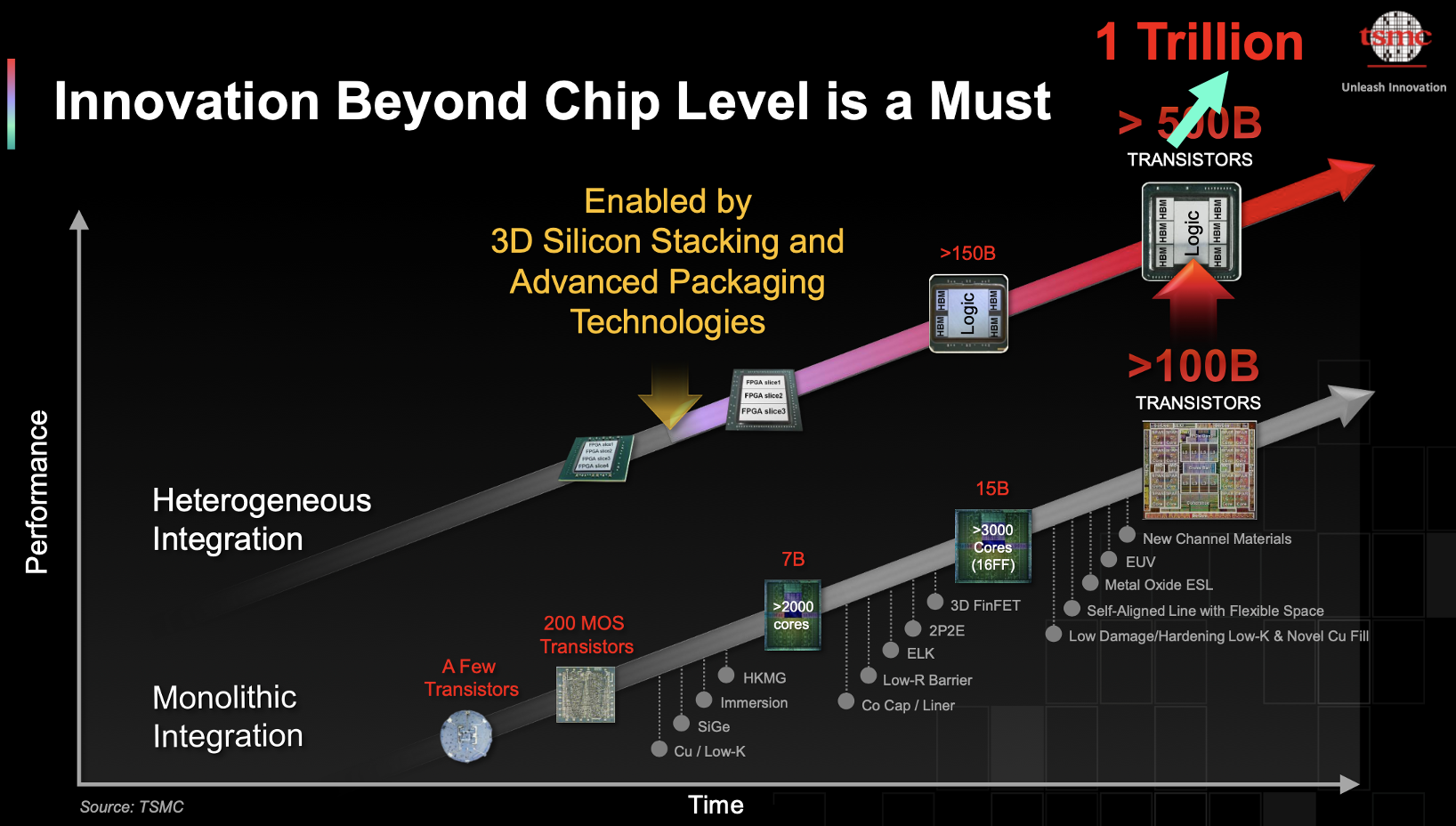
These trends have catalyzed a new era of exponential complexity increase, one that relies on heterogeneous integration of multiple dies (or chiplets) in a single package, and that has created the incredible focus and importance of advanced packaging as critical enabling technology. TSMC summarizes these trends nicely in the diagram below.
TSMC’s Advanced Packaging Technologies
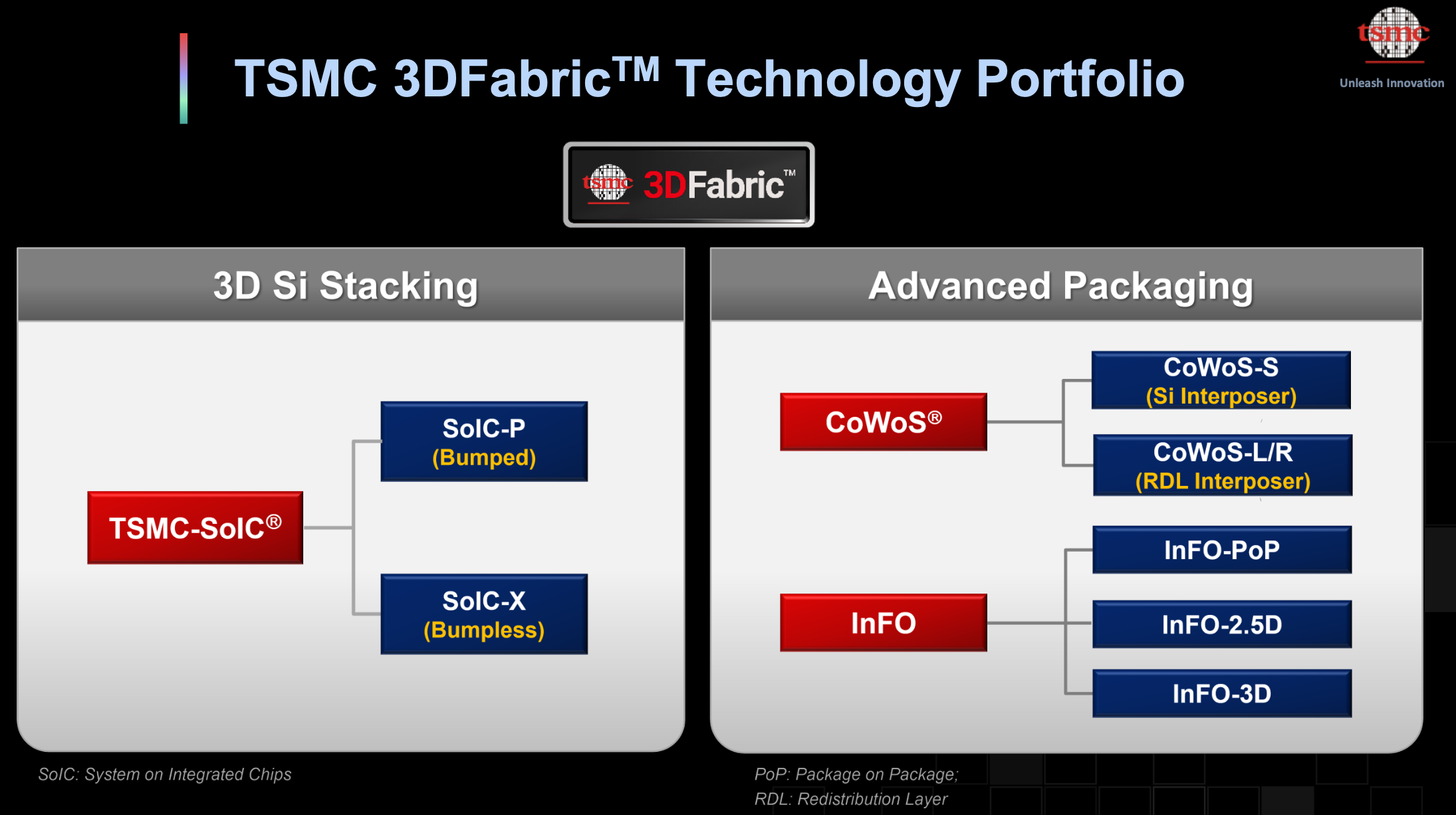
TSMC presented many parts of its strategy to support advanced packaging and open the new era of heterogenous integration. These are the technology building blocks for TSMC’s 3DFabric™ Technology Portfolio:
- CoWoS®: Chip-on-Wafer-on-Substrate is a 2.5D wafer-level multi-chip packaging technology that incorporates multiple dies side-by-side on a silicon interposer to achieve better interconnect density and performance. Individual chips are bonded through micro-bumps on a silicon interposer forming a chip-on-wafer (CoW).
- InFO: Integrated Fan-Out wafer level packaging is a wafer level system integration technology platform, featuring high density RDL (Re-Distribution Layer) and TIV (Through InFO Via) for high-density interconnect and performance. The InFO platform offers various package schemes in 2D and 3D that are optimized for specific applications.
- TSMC-SoIC®: Is a service platform that provides front-end, 3D inter-chip (3D IC) stacking technologies for re-integration of chiplets partitioned from a system on chip (SoC). The resulting integrated chip outperforms the original SoC in system performance. It also affords the flexibility to integrate additional system functionalities. The platform is fully compatible with CoWoS and InFO, offering a powerful “3Dx3D” system-level solution.
The figure below summarizes how the pieces fit together.
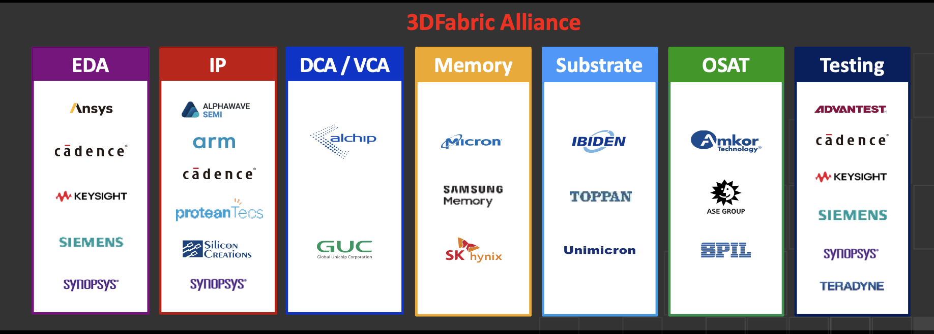
Getting all this to work across the ecosystem requires collaboration. To that end, TSMC has established the 3DFabric Alliance to enable work with 21 industry partners to cover memory, substrate, testing and OSAT collaborations to lower 3DIC design barriers, improve STCO and accelerate 3DIC adoption. The group also drives 3DIC development in tools, flows, IP, and interoperability for the entire 3Dfabric stack. The figure below summarizes the group of organizations that are involved in this work.
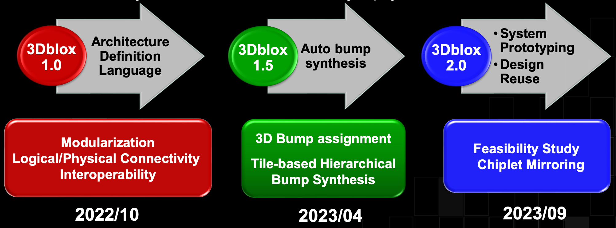
There is so much effort going on to support advanced packaging at TSMC. I will conclude with one more example of this work. 3Dblox™ is a standard new language that will help make designing 3D ICs much easier. TSMC created 3Dblox alongside its EDA partners such as Ansys, Cadence, Intel, Siemens, and Synopsys to unify the design ecosystem with qualified EDA tools and flows for TSMC 3DFabric technology. The figure below shows the progress that has been achieved with this effort.
To Learn More
I have touched on only some of the great work going on at TSMC to create advanced packaging solutions to pave the way for the next era of multi-die, heterogeneous design. You can get more information about this important effort at TSMC here. And that’s how TSMC advanced packaging overcomes the complexities of multi-die design.
Share this post via:


