Accelerate Semiconductor Fab Transformation with AWS | AWS for Industries – AWS Blog
The high-volume manufacturing of semiconductor devices relies on complex wafer production and packaging processes, supported by a long list of specialized equipment manufacturers and materials suppliers. This heterogenous and globally distributed manufacturing supply chain must work closely with semiconductor design and verification teams. These teams create application-specific integrated circuits (ASICS) and systems-on-chip (SoC) to meet performance, quality, and security requirements of industries including automotive, communications, and others. Increasing yield and optimizing costs require secure communication and collaboration on data gathered across all stages such as design, verification, and manufacturing.
Globally distributed semiconductor companies and their manufacturing partners increasingly rely on Smart Manufacturing technologies to improve operational efficiency and reduce time to market (TTM). These technologies include advanced production and yield analytics, Artificial Intelligence and Machine Learning (AI/ML), automated forecasting and supply chain risk analysis, industrial IoT, predictive maintenance, digital, analog, mixed-signal and EM/RF simulations, digital twins, customized manufacturing execution systems (MES), computational lithography, among others. At its core, Smart Fab is a data driven approach, allowing semiconductor manufacturers and their fabless customers to remain competitive in a dynamic and challenging market. This ensures efficient supply chain integration, improved transparency, security, traceability, and reliability.
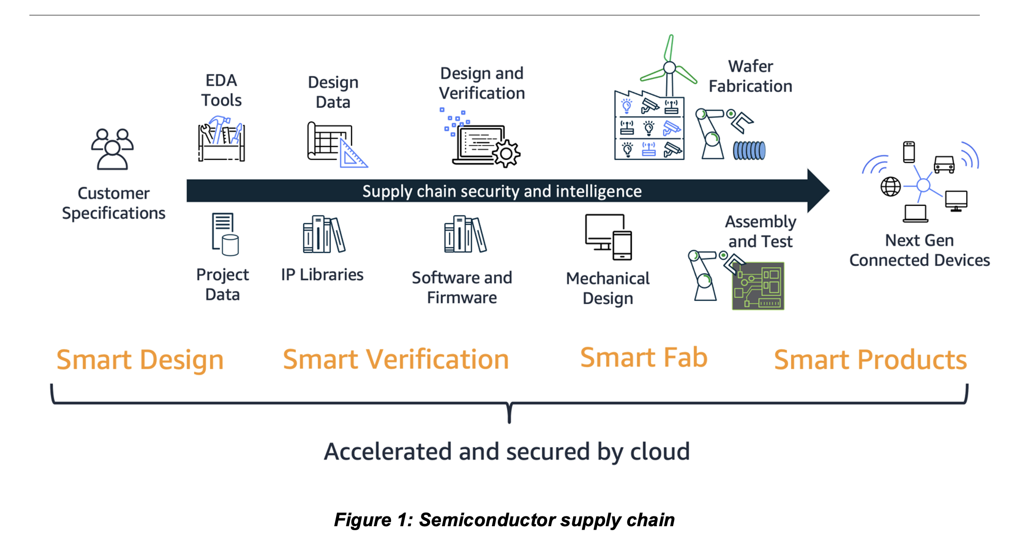
Smart Fab spans the entire semiconductor supply chain (Figure 1). From a semiconductor foundry’s perspective, it provides a holistic view of all the fab systems. Some of these systems include engineering and design data (EDA, PLM, CAD, CAE), operations data from manufacturing applications, and machine/sensor data. The combination of data from these systems provides the ability to analyze the interaction between process equipment manufacturing automation, supply chain, commercial management, facilities monitoring, and control.
Smart Fab also extends beyond today’s typical approach to optimize capital expenditure (CAPEX), time to market, design quality, and advanced technology device fabrication. It focuses on continuous operational expenditure (OPEX) improvements across all fab operations, in addition to CAPEX optimizations, TTM, and quality. Secure access to data throughout the supply chain makes this possible with cloud-based collaboration, Internet of Things (IoT) technologies, AI/ML, and advanced analytics.
Secure collaboration is a key feature for Smart Fab. For a foundry, the platform can increase collaboration by enabling controlled access to data with its key suppliers for ease of communication and accelerated service response times. This results in improved responsiveness, reliability, traceability, and quality. For a fabless or integrated semiconductor company and its ASIC and SoC development teams, Smart Fab allows a high level of visibility, using actionable data generated during the manufacturing and test processes. For example, enabling curated data generated during wafer fab, die sort, packaging, assembly, and test can be used to evaluate and improve wafer yields, and reduce device failure rates.
With applications for chain participants, the reduced cost of sensor technologies for IoT and the rapid development of AI/ML methods expand the possibilities to collect and act on large amounts of operational and real-time data. IoT enabled sensors can provide an inexpensive way to get additional inspection points throughout the manufacturing process compared to the conventional wired sensor approach. IoT technologies also provide a way to integrate and analyze collected data with existing systems, resulting in potential process improvements. For a foundry, this implies the integration of all its systems as part of the IoT platform with the fabless designer of the chip to further improve visibility, yield, and TTM.
AI/ML and Data Analytics are becoming an increasingly important productivity tool, reducing time to market across the semiconductor manufacturing value chain. Manufacturing, being the largest cost driver, will likely benefit the most from AI/ML and Data analytics in terms of cost reduction and productivity improvements. For example, AI/ML can be used to improve business processes such as forecasting, scheduling and inventory management, overall equipment effectiveness (OEE), process parameters, defect detection, and automated testing. Chip design and verification is another area that stands to gain from AI/ML and Data Analytics. Manufacturing-related analytics can be used at design stages to improve design-for-manufacturing and design-for-quality (“zero defect”) initiatives. It can reduce costly iterations for new products introductions and accelerate ramp-up time.
AWS enables Smart Fab through cloud-based services for AI/ML, Data Analytics, and IoT. These services accelerate and enhance semiconductor manufacturing capabilities by utilizing cloud infrastructure and can be tailored to meet specific requirements. Additionally, AWS for Industrials offers a set of solutions and services tailored for Industrial customers.
AWS has service offerings in the following key areas to drive a measurable impact:
Figure 2 shows the Data Analytics and AI/ML reference architecture for Smart Fab, and it illustrates a hybrid cloud framework from the foundry’s perspective. The Fab’s physical equipment, controllers, cameras, sensors, human-machine interfaces are latency sensitive and remain on-premises. Latency sensitive manufacturing applications can also be run on premises with AWS Outposts, which is a fully managed service that offers the same AWS infrastructure, AWS services, APIs, and tools within a data center.
Central to a Data Analytics and AI/ML strategy is the data lake in the cloud. Multiple data lakes may be managed by different organizations. For example, at a fabless semiconductor customer, fab and test partners can improve operations and increase device yields by analyzing data captured from field deployments in combination with manufacturing and design-related data. To ingest data from sensors, machines, and manufacturing applications running on-premises or in the cloud, AWS offers a variety of services (AWS IoT Greengrass, AWS IoT SiteWise, Amazon Kinesis, AWS Transfer for SFTP). The data from these sources are ingested, contextualized and then stored in the data lake. The architecture can also be optimized for collaboration with a semiconductor design environment running on AWS. Relevant design data is sent to the foundry, on-premises test facility, and data lake. Data lake serves as a central source of all fab data for analytics applications, advanced ML modeling and advanced AI services to generate actionable insights.
AWS for Smart Fab provides a customizable blueprint to address different use cases and the different needs of semiconductor companies. By using AWS services, a Smart Fab can apply advanced tools to data across the entire supply chain in near-real-time, proactively correcting potential issues and improving yield. Augmenting human intelligence with advanced analytics and AI/ML uncovers the underlying trends and creates new opportunities to improve semiconductor manufacturing cycles.
Improvements in both CAPEX and OPEX are necessary for all semiconductor manufacturers to increase profitability and growth within the highly competitive and dynamic semiconductor market environment built on the challenges of diverging products, technologies, and client base. Efficient supply chain integration is critical given that it faces restrictions in terms of experienced expert resources (for both operation and maintenance) and the availability of spare parts and consumables. Smart Fab provides opportunities for supply chain integration, improves transparency, reliability, sustainability of the facility systems, reducing OPEX. Ultimately, the operational data from existing fab, packaging, and assembly lines can be used in comparative analysis to optimize CAPEX for new projects, improve development turnaround times, and increase new product introduction (NPI) cycles.
Click here to learn more about Semiconductor and Electronics on AWS
Follow “Semiconductor and Electronics” on the AWS for Industries blog
Erick is a Solutions Architect at Amazon Web Services focusing on clients in the Semiconductors and Electronics industry. He works closely with customers to understand their business challenges and identify how AWS can be leveraged to achieve their strategic goals. His work has primarily focused on projects related to Artificial Intelligence and Machine Learning (AI/ML). Prior to joining AWS, he was a Senior Consultant at Deloitte’s Advanced Analytics practice where he led workstreams in several engagements across the United States focusing on Analytics and AI/ML. Erick holds a B.S. in Business from the University of San Francisco and an M.S. in Analytics from North Carolina State University.
Mark Duffield is Worldwide Tech Lead for Semiconductor and Electronics at Amazon Web Services. He travels around the world working with semiconductor companies to enable workflows on AWS. He frequently speaks at industry and AWS events discussing architectural designs, market trends, and AWS features and services. He has deep experience with electronic design automation, high performance computing, enterprise software development, and distributed file systems.
Nishant Saini is a Principal Partner Solutions Architect at AWS for Industrial Software and Semiconductor segment. Nishant works closely with AWS partners acting as a trusted advisor to define, build and evangelize cloud-based solutions for manufacturing and semiconductor industry. He has expertise in industrial automation, industrial data platforms, cybersecurity and supply chain. He is passionate about leveraging technology to advance the state of the manufacturing industry.


