Bao bì 2.5D: Hướng dẫn cơ bản
Imagine a world where electronic devices are exponentially more powerful yet astonishingly compact. This is the promise of 2.5D packaging, an innovative approach to semiconductor design. It’s reshaping the landscape of computing, from smartphones to servers.
In the realm of electronics, understanding the building blocks is key. 2.5D packaging is not a mere upgrade but a transformative leap, offering benefits such as improved performance, enhanced power efficiency, and a higher integration density, pivotal for today’s high-demand applications.
Get ready to embark on a journey through the intricate world of 2.5D packaging. We will delve into its vital role in semiconductor manufacturing, explore the key technologies enabling this advancement, address the challenges it poses, highlight recent innovations, and speculate on its transformative future.
What is a 2.5D Package?
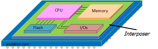
2.5D packaging is an advanced packaging technology that represents an intermediary evolutionary step between traditional 2D and more complex 3D packaging systems. Unlike 3D packaging, where silicon chips are stacked vertically and interconnected with through-silicon vias (TSVs), 2.5D packaging employs a silicon interposer—a flat substrate that sits between the silicon chips and the mounting surface.
The silicon interposer is etched with fine wiring patterns, providing high-bandwidth interconnections between different chips mounted on its surface. Key advantages of 2.5D packaging over conventional 2D packaging include improved power consumption and power efficiency due to shorter connectivity distances, enhanced signal integrity owing to reduced wiring lengths, and higher integration densities.
This innovative packaging solution allows semiconductor manufacturers to combine heterogeneous silicon chips (such as CPUs, GPUs, and memory chips) within a single package, offering enhanced performance characteristics like increased bandwidth memory access and reduced power densities.
Integration technologies like 2.5D packaging are a testament to the incessant drive for miniaturization and performance optimization in electronic devices. They present a compromise between improved performance and manageable manufacturing complexity compared to full-scale 3D integration, making them a pragmatic choice for current-generation semiconductor devices.
|
Interposer |
Silicon substrate used to interconnect multiple chips |
|
Power Efficiency |
Reduced power consumption due to optimized chip layout |
|
Performance |
Greater bandwidth and signal integrity |
|
Level of Integration |
Heterogeneous integration of different types of silicon |
|
Manufacturing Complexity |
Less complex than 3D packaging, but more than traditional 2D packaging |
Benefits of 2.5D Packaging
2.5D packaging technology serves as a pivotal juncture in the evolutionary trajectory of semiconductor packaging, effectively bridging the gap between the plateau of traditional 2D layouts and the aspirational zenith of full 3D integration. The multitude of benefits it provides encompasses various spectra of performance metrics, integration principles, and power management protocols, positioning it as a premier choice for semiconductor manufacturers striving for a synergy of complexity management and performance enhancement.
|
Signal Integrity Improvement |
Minimizes parasitic capacitance and inductance |
|
Enhanced Bandwidth Memory Access |
Facilitates higher data transfer rates between chips |
|
Microelectronic Miniaturization |
Enables smaller, more compact multi-chip packages |
|
Heterogeneous Integration Capability |
Combines diverse functional blocks such as CPU, GPU, memory |
|
Thermal Management |
Offers efficient heat dissipation mechanisms |
|
Supply Chain Diversification |
Simplifies inventory due to integration of multiple chips |
Improved Performance
The quest for optimal system performance in the world of electronic devices invariably ends at the doorstep of the packaging technology employed. 2.5D packaging, with its advanced interconnect framework provided by the silicon interposer, fosters a milieu where optimum signal integrity is maintained—a crucial factor in minimizing latency and boosting system speed. This also results in an associated decrease in parasitic capacitance and inductance, hence preserving the integrity of high-speed signals traversing the interposer’s microscopic pathways. Moreover, the capacity for higher bandwidth memory access is testament to 2.5D packaging’s capability to address insatiable demands for faster data processing and transfer rates.
Higher Integration Density
Embarking on the incorporation of various silicon chips within a singular envelope, 2.5D packaging synergizes the wealth of talents presented by different semiconductor technologies, from microprocessors to memory dies. This heterogeneity fosters an unparalleled level of integration density, permitting electronic devices to house a compact yet potent confluence of capability and complexity. By leveraging this integration, device manufacturers gain the latitude to produce slimmer and more lightweight products without compromising computational power—a compelling narrative in today’s space-constrained applications.
Enhanced Power Efficiency
The advantages of 2.5D packaging extend unequivocally to the domains of power consumption and supply. By optimizing the layout of chips within the proximity permitted by the silicon interposer, the power consumption undergoes a significant reduction as the signal transit distances are curtailed, leading to a precipitous fall in power densities. The precision with which power can be distributed across the integrated chips within the 2.5D package further elucidates the efficacy of this technology in achieving enhanced power efficiency, which in turn leads to extended battery life in portable electronic devices and mitigation of heat-related challenges.
The Role of 2.5D Packaging in Semiconductor Manufacturing
2.5D Packaging has catalyzed a transformation within the realm of semiconductor manufacturing, offering a paradigm where the limitations of planar (2D) integration are transcended without incurring the structural complexities and economical implications of full 3D packaging. As an interstitial evolutionary step, 2.5D packaging technology leverages the elevated surface area offered by Silicon Interposers to enable Vertical Stacking and Signal Integrity preservation, pivotal for addressing the burgeoning signal routing challenges as semiconductor devices scale down in size. It is at the nexus of increased circuit density and requirement for faster inter-chip communication that 2.5D assumes its cardinal role—essentially expanding the real estate for electronic pathways, while minimizing interconnect length and latency.
|
Vertical Stacking |
Allows for a denser circuit layout with reduced interconnect length |
|
Silicon Interposers |
Facilitates high-density routing between stacked dies |
|
Signal Integrity Preservation |
Mitigates crosstalk and electromagnetic interference |
|
Heterogeneous Integration |
Enables the combination of different chip technologies in one package |
|
Thermal Efficiency |
Provides an architecture conducive to effective heat dissipation |
|
Power Efficiency |
Reduces overall power consumption through design optimization |
By interlacing the collective strengths of Silicon Via technology, fan-out wafer-level packaging, and seamless integration of disparate chip functionalities, 2.5D packaging is embraced by semiconductor manufacturers as a means to propel electronic devices toward new pinnacles of performance and power efficiency.
Integration of Different Components
Integration is a linchpin of contemporary electronic device sophistication, so the capability to condense multiple components into a single package stands as a significant benefit of 2.5D technology. Semiconductor packaging technology has been proactively finessed to enable single packages containing CPUs, GPUs, and memory chips, among others—each serving distinct and pivotal roles within an electronic circuit. This tapestry of integration is actualized through the use of a Silicon Interposer, which acts as a bedrock upon which disparate silicon chips are laid, connected by a network of silicon vias ensuring high-speed electrical connectivity. This intricate orchestration accords semiconductor manufacturers the versatility to enhance bandwidth memory capabilities, optimize power supply distribution, and mitigate power densities—all while securing the escalation of power efficiency and signal integrity across the 2.5D package.
|
Optimized Performance |
CPUs, GPUs, DRAM |
|
Power Consumption Reduction |
Power Management Integrated Circuits (PMICs) |
|
Space Conservation |
Multi-function System-on-Chips (SoCs) |
|
High-Speed Connectivity |
High Bandwidth Memory (HBM) |
|
Improved Thermal Management |
Thermally Advanced Packaging (TAP) |
|
Simplified Inventory and Supply Chain |
Combined assembly reducing parts inventory |
Integration of Heterogeneous Technologies
The true genius of 2.5D packaging manifests in its capacity for Heterogeneous Integration—the seamless fusion of different technological paradigms within a unified architecture. This facet of advanced packaging technology is foundational in reconciling the disparate thermal, electrical, and physical characteristics endemic to various silicon chips. Leveraging advanced techniques, it amalgamates silicon wafers that may differ in function, performance metrics, or power profiles into a coherent and optimized assembly, enabling semiconductor manufacturers to construct a layered vista of functionalities that would be unachievable with homogenous technologies.
|
Thermal Disparity |
Efficient thermal interfaces and interposer designs |
|
Varied Operating Voltages |
Advanced power management techniques |
|
Divergent Signal Frequencies |
Optimized routing and connectivity solutions |
|
Physical Size Variations |
Customizable interposer layouts |
Encompassing integration densities that significantly reduce the need for external interconnects, this level of integration is advantageous for compact system designs, enhancing integration technologies and introducing a confluence of capabilities that elevate the functionality of the next wave of electronic devices. As such, 2.5D packaging is a fulcrum atop which the leverage of enhanced computational capacity, signal integrity, and integration density pivots, thereby anchoring the progression of advanced semiconductor packaging techniques.
Key Technologies for 2.5D Packaging
As the semiconductor industry strives for greater power efficiency and signal integrity, 2.5D packaging stands as a formidable solution. Crucial to this approach are several key technologies, each contributing its own vital aspect to the augmentation of electronic devices. Prominent among these technologies are the Silicon Interposer, enabling high-density interconnections; Vertical Stacking, which maximizes component density; and a suite of Advanced Packaging Techniques, promoting higher levels of chip integration and functionality. These components synergize, giving 2.5D packages their superior performance attributes.
These technologies collectively forge the backbone of 2.5D packaging, facilitating enhanced integration densities and offering semiconductor manufacturers a powerful toolkit to meet the ever-increasing demands of modern electronic devices.
Silicon Interposer
The Silicon Interposer is pivotal to the implementation of 2.5D packaging. Serving as a bridge between the silicon dies and the substrate, interposers afford high-density interconnects that allow for lower power consumption and higher bandwidth than traditional wire-bond or flip-chip connections. Key attributes of Silicon Interposers include:
- Material Compatibility: The thermal expansion properties closely match those of silicon chips, minimizing stress during temperature cycles.
- Customizability: Can be tailored with through-silicon vias (TSVs) and redistribution layers (RDLs), fitting various circuit architectures.
- Electrical Performance: Provides a shorter path for signal transmission, which enhances signal integrity and reduces latency.
Vertical Stacking
Vertical Stacking emerges as a crucial approach within 2.5D packaging, characterized by aligning multiple silicon dies atop one another, employing TSVs for internal connections. Benefits of this dense layout manifold, including:
- Circuit Real Estate: Achieves remarkable circuit miniaturization, crucial in the realm of portable and wearable technology.
- Improved Bandwidth: Minimizes the distance electrical signals must travel, enhancing the speed of data transfer.
- Thermal Considerations: Innovative heat dissipation techniques become imperative, demanding sophisticated thermal interface materials and heat spreader designs.
Advanced Packaging Techniques
Advanced packaging techniques intrinsic to 2.5D integration encompass a broad array of strategies, each playing a distinct role in overall device performance. These techniques include:
- Fan-Out Wafer-Level Packaging (FOWLP): Facilitates expansive I/O counts and allows for additional components, like passives or antennas, to be incorporated within the same package.
- Heterogeneous Integration: Combines dissimilar technologies, such as analog, digital, RF, and optoelectronics, within a single package, optimizing functionality without compromising form factor.
- Thermal & Power Management: Both are optimized through innovative package designs that address the heat dissipation challenges and power distribution needs of modern high-performance chips.
Together, these advanced techniques represent a multidisciplinary convergence of materials science, electrical engineering, and mechanical design, enabling the future-forward design of semiconductor devices powered by the potential of 2.5D packaging.
Challenges in 2.5D Packaging
While 2.5D packaging presents significant advancements in semiconductor manufacturing, it also introduces a set of distinctive challenges. Addressing these requires innovative strategies and a deep understanding of the interplay between chip architecture and packaging technology. From the complexities of manufacturing to heat management and maintaining signal integrity, semiconductor manufacturers face formidable hurdles in tapping into the full potential of 2.5D packaging.
Manufacturing Complexities
The construction of 2.5D packages poses intricate geometrical and material challenges that extend well beyond the capabilities of conventional packaging techniques. Key elements of the manufacturing process include:
- Precision Alignment: Critical for the proper functioning of interposers, silicon chips, and through-silicon vias (TSVs). Any misalignment can disrupt signal transmission and impact overall device performance.
- Assembly Yield: The rate of successfully assembled devices vs. the total number manufactured is a crucial metric that can significantly affect cost-efficiency due to the multiplicity of interconnected components.
- Cost Factors: Advanced tools and materials—such as high-quality interposers and the implementation of TSVs—can elevate production expenses, impacting the economic viability for certain applications.
- Qualification Processes: Comprehensive testing protocols are essential to ensure that every integrated circuit meets stringent performance standards, adding additional layers of complexity and requisite scrutiny to the fabrication process.
Heat Dissipation
The vertical stacking of ICs in 2.5D packaging can exacerbate thermal challenges, as heat generation is concentrated within a smaller footprint. Efficient thermal management is, therefore, critical:
- Thermal Interface Materials (TIMs): Essential for improving the thermal contact between components and heat sinks or spreaders, TIMs must be carefully selected to optimize heat transfer.
- Heat Spreader Design: Custom-designed for each unique package architecture, heat spreaders play a vital role in dispersing thermal energy away from hotspots.
- Cooling Solutions: Depending on the application, active or passive cooling methods may be necessary. Advanced solutions, such as liquid cooling, may be integrated to manage extreme temperatures.
Interconnect Lengths and Signal Integrity
Signal integrity is paramount in electronic devices, and it directly correlates with interconnect lengths. In 2.5D packaging, the spatial rearrangement of components affects this critical factor:
- TSVs and RDLs: Although through-silicon vias and redistribution layers curtail interconnect lengths and help preserve signal integrity, their precise implementation is technologically demanding.
- Electromagnetic Interference (EMI): With components in closer proximity, EMI can become a notable concern affecting signal quality and necessitating EMI shielding solutions.
|
Interconnect Length |
Shorter pathways desired for signal strength |
Longer distance can degrade signal |
|
Crosstalk |
Signal interference between adjacent wires |
Can distort or alter information |
|
EMI |
Electromagnetic waves affecting signal paths |
Causes potential data corruptions |
|
Shielding |
Reduces EMI influence |
|
Differential Signaling |
Minimizes crosstalk impact |
|
TSVs/RDLs |
Shortens path, maintains signal quality |
In summary, as semiconductor manufacturers forge ahead with 2.5D packaging, addressing these manufacturing complexities, heat dissipation challenges, and signal integrity issues will be instrumental in advancing 2.5D packaging’s viability and widespread adoption.
Advancements in 2.5D Packaging
The landscape of semiconductor packaging has seen significant evolution with the advent of 2.5D packaging, an advanced packaging technology providing enhanced performance through a high level of integration. One of the pivotal advancements in 2.5D packaging is the implementation of silicon interposers, which act as bridges facilitating connections between silicon chips. This technology has markedly improved the integration density of packages and allows for the integration of heterogeneous chips with diverse functionalities into a single package.
|
Silicon Interposer |
Higher bandwidth, improved power efficiency |
|
Redesigned TSVs |
Reduced power consumption, increased reliability |
|
Enhanced RDL |
Optimized signal integrity, minimized latency |
|
Thermal Solutions |
Managed power densities, prolonged device lifespan |
In addition to these improvements, there have been strides in fine-pitch ball grid array (FBGA) technologies, as well as in the design of micro-bumps and copper pillars that establish robust physical and electrical connections with minimized resistance and inductance. These advancements collectively contribute to the overall performance and reliability of electronic devices, especially where high bandwidth memory and rigorous computation needs are pivotal.
Advanced Semiconductor Packaging Technologies
Advanced semiconductor packaging technologies have been instrumental in meeting the demands for increased performance and power efficiency in electronic devices. Heterogeneous integration technology allows for the coalescing of differently purposed dies — such as logic, memory, and analog chips — into a comprehensive system within a single package. This level of integration offers significant benefits in terms of shorter interconnect distances and reduced latency.
Semiconductor manufacturers employ advanced packaging techniques such as Fan-Out Wafer-Level Packaging (FOWLP) and 3D integration to increase the functionality and performance of semiconductor devices while keeping their size compact. FOWLP extends the available I/O density beyond the size of the chip, which is critical for applications where space constraints are critical. Meanwhile, 3D integration vertically stacks dies, enabling higher performance and reduced power consumption compared to traditional 2D layouts.
5D & 3D IC Packaging
The term “5D packaging” is not a well-established concept in semiconductor manufacturing, which traditionally discusses advancements in terms of 2.5D and 3D packaging. 3D Integrated Circuits (ICs) represent the next frontier beyond 2.5D packaging, leveraging vertical stacking and through-silicon vias (TSVs) for inter-die connections to further minimize signal delays and power losses. Silicon vias play a central role in these integration technologies, piercing through the silicon wafers to establish inter-layer connections that boast minimal latency and high speed.
3D IC packaging pushes the boundaries of integration density and efficiency, leading to a quantum leap in performance for a variety of semiconductor applications. However, it also amplifies challenges in areas such as heat management and interconnect yield, heightening the importance of advanced thermal interfaces and reliable manufacturing processes.
Chip on Wafer on Substrate (CoWoS)
Chip on Wafer on Substrate (CoWoS) is a key technique within the landscape of 2.5D integration technologies, which involves the assembly of known good dies on a silicon interposer wafer before mounting the ensemble onto a substrate. CoWoS solutions address several challenges inherent to advanced packaging such as signal integrity, power supply management, and integration density.
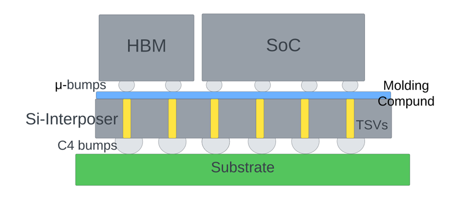
CoWoS technology is characterized by its ability to interconnect multiple high-performance chips using TSVs and micro-bumps, facilitating high-speed and energy-efficient communication between the chips. This integration method is particularly advantageous for applications requiring vast computational power and data-processing capabilities, such as high-performance computing and networking systems.
Overall, the continuous progression of advanced packaging technologies like 2.5D packaging is driving innovations that will support the next generation of electronic devices, catering to the relentless demand for more power-efficient, high-performing, and compact solutions.
Emerging Applications for 2.5D Packaging
The relentless drive towards miniaturization and performance enhancement in the semiconductor industry has led to the proliferation of 2.5D packaging across a myriad of emerging applications. As engineers and designers push the boundaries of electronic device capabilities, 2.5D packaging emerges as a vital technology, instrumental in enabling the next leap in computational speed, efficiency, and complexity.
|
Artificial Intelligence |
Enhanced compute density for neural networks |
|
Quantum Computing |
Improved interconnectivity for quantum processors |
|
Edge Computing |
Reduced latency, increased bandwidth for distributed networks |
|
Wearables |
Greater integration density in constrained form factors |
Each of these domains benefit exquisitely from the power and space efficiency gains afforded by the advanced packaging technology of 2.5D, as it accommodates a higher integration of diversified silicon die within a single package, thereby reducing signal travel time and energy dissipation while optimizing real estate usage.
High-Performance Computing
In high-performance computing (HPC), the demands for speed and efficiency are relentless. The integration of 2.5D packaging technology in HPC systems provides a transformative improvement over traditional monolithic designs. Through the strategic placement of heterogeneous components such as CPUs, GPUs, and specialized accelerators onto a singular silicon interposer, 2.5D packaging bolsters the throughput of interconnects, thus scaling up computational prowess while maintaining or decreasing power consumption.
- Critical Benefits for HPC:
-
- High-bandwidth memory (HBM) integration for rapid data access
- Improved thermal management through sophisticated heat dissipation techniques
- Shorter inter-die connections, leading to faster signal transmission and reduced latency
The aggregation of these factors through 2.5D packaging ensures that HPC can meet the increasing demands of complex simulations, cryptographic analysis, and large-scale data processing tasks.
Memory Interfaces
At the heart of advancing memory interfaces lies 2.5D packaging technology. This advanced packaging paradigm empowers memory chips, such as high bandwidth memories (HBMs), to operate with unprecedented data transfer rates and lower power consumption in comparison to traditional memory solutions.
The juxtaposition of HBMs alongside logic dies on an interposer dramatically enhances the bandwidth available to processors, ushering in a new era for high-speed computing applications. This synergy optimizes the performance of data-intensive tasks such as real-time analytics, 4K and 8K video processing, and complex scientific computations.
- Key Improvements in Memory Interfaces:
-
- Bandwidth expansion through vertical chip stacking and a wider interface
- Signal integrity preservation due to reduced interconnect length
- Proliferated adoption in graphics, network infrastructure, and data centers
Internet of Things (IoT)
IoT is synonymous with vast networks of connected devices that often require low power consumption and the capacity to process and transmit data efficiently. 2.5D packaging presents a groundbreaking method to house diverse sensor technologies, control units, communication modules, and power management systems within a constrained space.
- Advantages for IoT Applications:
-
- Advanced integration enabling the convergence of heterogeneous functionalities
- Reduced power profiles, essential for battery-operated and remote devices
- Superior reliability for sustained operation in varied environments
As IoT ecosystems scale in complexity and scope, 2.5D packaging becomes increasingly instrumental, offering the miniaturization and integration needed for the next wave of smart cities, connected vehicles, and personalized healthcare technologies.
The ongoing refinement and adoption of 2.5D packaging stand as testimony to its critical role in shaping the future across a spectrum of computing paradigms, from ubiquitous embedded devices to supercomputing behemoths. As we look ahead, 2.5D packaging continues to redefine the landscape of semiconductor integration, driving unprecedented advancements in electronic systems and applications.
Future Trends in 2.5D Packaging
The trajectory of 2.5D packaging technology is skewed toward enabling highly sophisticated, next-generation electronic devices with a keen focus on achieving superior computational power and energy efficacy. Anticipating future trends, we envision several driving factors that will spur innovation and enhancement within this domain.
One core trend resides in amplifying the level of integration, packing a crescent number of functionalities into single-package solutions, thus pushing integration density to new heights. Another is bound in the perpetual advancements of process technologies that pave the way for more refined and intricate manufacturing, reducing feature size while increasing the yield and reliability of packaging.
Moreover, as power densities soar, the need for enhanced thermal performance becomes paramount, dictating innovations in heat dissipation techniques. Each of these trends not only encapsulates the direction of 2.5D package enhancements but collectively converges to redefine the very standards of semiconductor packaging technology.
Increasing Integration Density
The evolution of 2.5D packaging is centered upon aggrandizing the level of integration, where the promise of embedding an expanding suite of heterogeneous components within a silicon interposer frames the impending advancement. This progression leads to a potent surge in integration density, enabling highly functional, compact systems that elicariate significant performance boosts.
|
Silicon interposers |
Utilization of nanoscale features to accommodate more die |
|
Through-Silicon Vias (TSVs) |
Densification to provide superior I/O capabilities |
|
Die stacking |
Enhanced vertical integration, leveraging interposer to support more layers |
|
Package footprints |
Reduction due to increased die density, optimizing space on PCBs |
As semiconductor manufacturers inaugurate these techniques, we can prognosticate an era where single packages actuate a multitude of compute, memory, and sensor capabilities, once relegated to disparate chips.
Advancements in Process Technologies
With the relentless progression in integration capabilities, 2.5D packaging technologies are also subjected to continuous enhancements in process technologies. Manufacturers must leapfrog current limitations by developing bespoke lithographic techniques, chemical-mechanical polishing (CMP), and advanced bonding methods to fabricate finer, yet resilient, package structures.
- Innovations include:
-
- Sub-micron lithography for ultra-precise interposer patterning
- Next-generation TSV etching and filling processes for improved uniformity
- Implementation of AI & Machine Learning for process optimization
- Extending the frontiers of wafer-level packaging (WLP) and fan-out WLP
These process evolutions will undoubtedly fuel the attainment of unprecedented power efficiency, signal integrity, and reliability within 2.5D packaged devices.
Enhanced Thermal Performance
As we strive towards greater integration and performance peaks, the thermal envelope of 2.5D packaged components tightens. Advances in thermal interface materials (TIMs), along with novel
cooling architectures, are paramount to mitigate the associated rise in junction temperatures.
- Thermal performance must be addressed through:
-
- Development of high-conductivity TIMs to improve die heat spreading
- Innovation in passive and active cooling solutions tailored for 2.5D constructs
- Enhanced mold and underfill materials to bolster thermal stability
By integrating these advanced thermal management solutions, semiconductor packages can deliver robust performance without succumbing to thermal throttling, ensuring the longevity and reliability of high-power-density devices in a vast array of applications.
As we look to the horizon, 2.5D packaging is set to champion a transformative impact, furthering the advent of compact, reliable, and high performing electronic devices. The blend of heterogeneous integration technology, breakthroughs in process technologies, and quelling the heat flux within dense package architectures augurs a resplendent future for this advanced packaging technique.