Clash of the Foundries: Cổng xung quanh + Sức mạnh phía sau ở 2nm
TSMC won FinFET. All noteworthy leading edge logic designs, even Intel’s, are manufactured on TSMC’s N5 and N3 process in southern Taiwan. Competitors have been left in the dust. Samsung has had poor performance and poor yields since their 7nm, Intel is still early in its journey to recovery with Intel 4 and 3; neither have major external or internal customers ordering on these nodes in volume.
Future dominance is not guaranteed for TSMC. FinFETs, cannot scale further and SRAM shrink has been dead for a few nodes. The industry is at a crucial inflection point. Leading-edge logic must adopt two new paradigms in the next 2-3 years: gate all around (GAA) and backside power delivery (BSPDN or backside power delivery network).
Intel fell apart with their 10nm node and lost their 3 year lead for a number of reasons including not adopting EUV and transitioning to cobalt metallization with an immature tool supply chain despite warnings from Applied Material that their tools were not ready. The new paradigms of GAA and BSPDN present new opportunities in the foundry pecking order. They could even potentially open the door to a new entrant to the space – Rapidus, the Japanese government backed 2nm foundry startup.
As the capital expenditures needed to build leading edge fabs skyrockets, this means either Samsung or Intel could be forced to drop out of the race. Below we’ll discuss these topics in detail: a deep dive into BSPDN tech followed by leading edge logic roadmaps from all four foundries, competitiveness of their process technologies, SRAM scaling, and our model of 2nm capex and wafer fab equipment (WFE) spend.
Gate All Around is not new. According to Samsung it has been in high volume production for a couple years, but the reality is that this is only in a single low volume bitcoin mining chip that doesn’t have any SRAM. The gate all around architecture is important topic given that all leading-edge nodes will use it from 2nm through the end of the decade. We’ve covered the transistor change in these two previous reports, these are a great starting place if you need a refresher:


Alongside gate all around transistors, BSPDN is the other key innovation in the next generation logic process technologies. In all current digital logic process technology, first transistors are fabricated on the wafer before dozen of metal layers are fabricated which bring power to the transistors and route signals between them and the outside world.
Scaling circuits mean both the transistors and the interconnects must shrink. In the past this was almost an afterthought, but scaling interconnects has become more difficult then scaling transistors. For example, more than 90% of EUV lithography is actually used on interconnects (contacts, vias, and metal layers), not the transistor layer itself. Along with decreasing the physical dimensions of the wires themselves, more transistors on a chip mean more interconnects. This drove a steady growth in the number of interconnect layers required. More layers mean higher fabrication costs, difficulty in routing design, and lower performance as signal paths get longer.
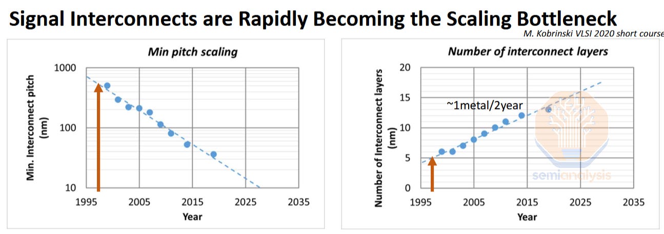
This didn’t mean the industry stopped progressing. Materials innovations, design technology co-optimization (DTCO), and EUV lithography drove interconnect scaling to today’s current process nodes. But as that playbook becomes more increasingly more expensive and limits continued shrinking. The calculus of implementing BSPDN is starting to make sense. It’s not a new idea, just one whose time has come. And it’s about time for innovation in interconnects, it’s been almost 30 years since the last evolution of interconnects, which was the shift from aluminum to copper in 1997.
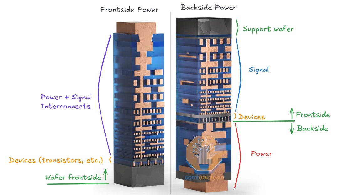
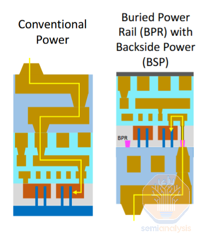
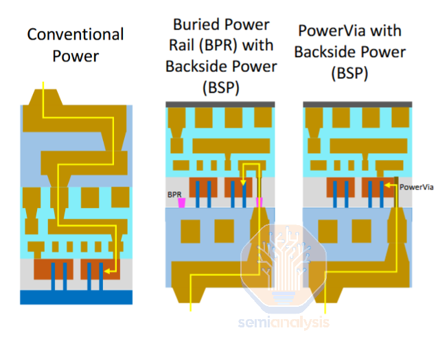
The core idea of BSPDN is to move the wiring for power to the backside of the wafer. It opens up breathing room for signal routing, which stay on the frontside, and power which is moved to the backside. Architecturally, this means that standard cells shorter than 6T (track) are more feasible. 6T refers to the cell height of standard cells which are the basic building blocks of digital logic, such as a NAND gate, and the height of the cell is commonly measured as a multiple of T, the number of Metal 2 wires or “Tracks” the cell spans. Shorter is better: smaller cells enable increased density without scaling the underlying features such as fins, gates, and metal interconnects. Scaling more features is expensive because it requires better lithography.
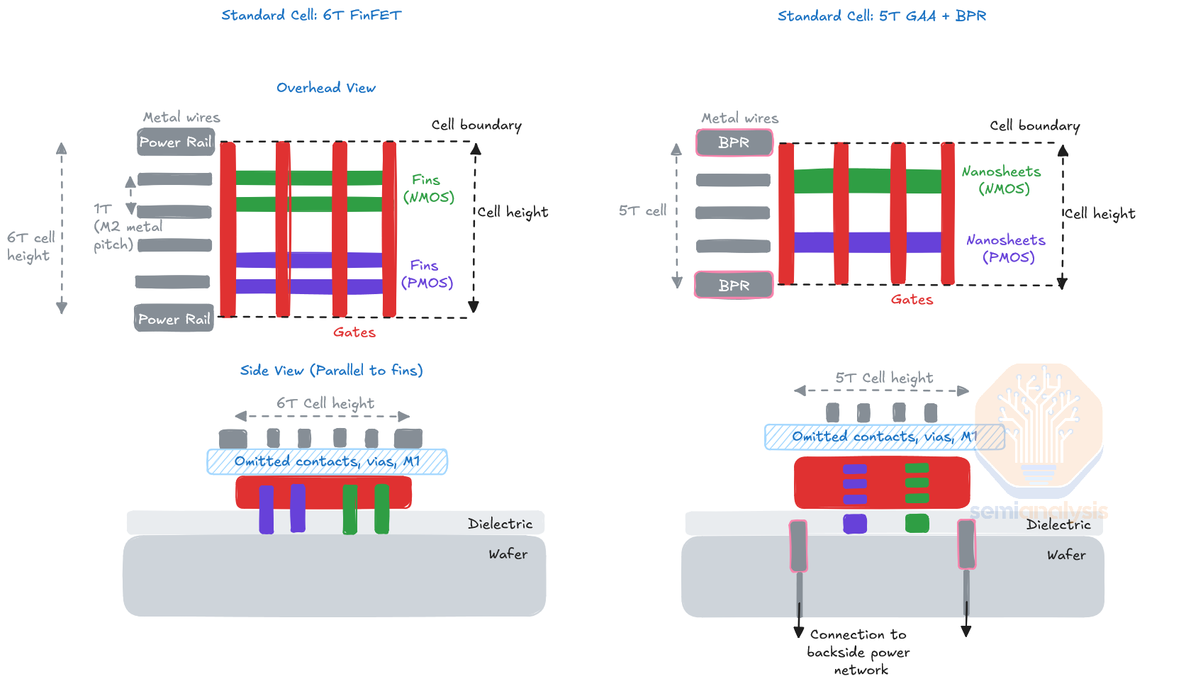
Viewed from overhead, the top and bottom of a standard cell are bound by wide metal rails in the M2 metal layer. These rails supply power and reference voltage to the cell and are connected to the rest of the power delivery network in higher metal layers. These rails are part of the total 6T height of typical frontside-only cells – moving them to the backside means the cell can be shrunk to 5T or shorter.
Power delivery also improves on two fronts with BSPDN. First, the length of the interconnect supplying power to the transistors is considerably shortened. Frontside-only power delivery at a 3nm node must traverse 15+ metal layers whereas backside power might include fewer than 5 layers and with much thicker (lower resistance) wires. The power loss from line resistance thus can be reduced by roughly an order of magnitude.
Second, BSPDN lessens the need for aggressive interconnect scaling. Resistance in copper wires increases exponentially as its diameter shrinks in the regime below 100nm. And now with leading edge now well below 20nm wire width, resistance is a critical issue.. This is undesirable as high line resistance wastes power and generates excess heat in the chip. It’s not a permanent solution – scaling will continue, and Cu alternatives will also be needed – but BSPDN offers relief.
Altogether BSPDN offers roughly 15-20% improvement in power usage versus a similar frontside-only process on high performance designs.
There are three distinct approaches being explored and/or implemented for backside power delivery: buried power rail, power via, and backside contact.
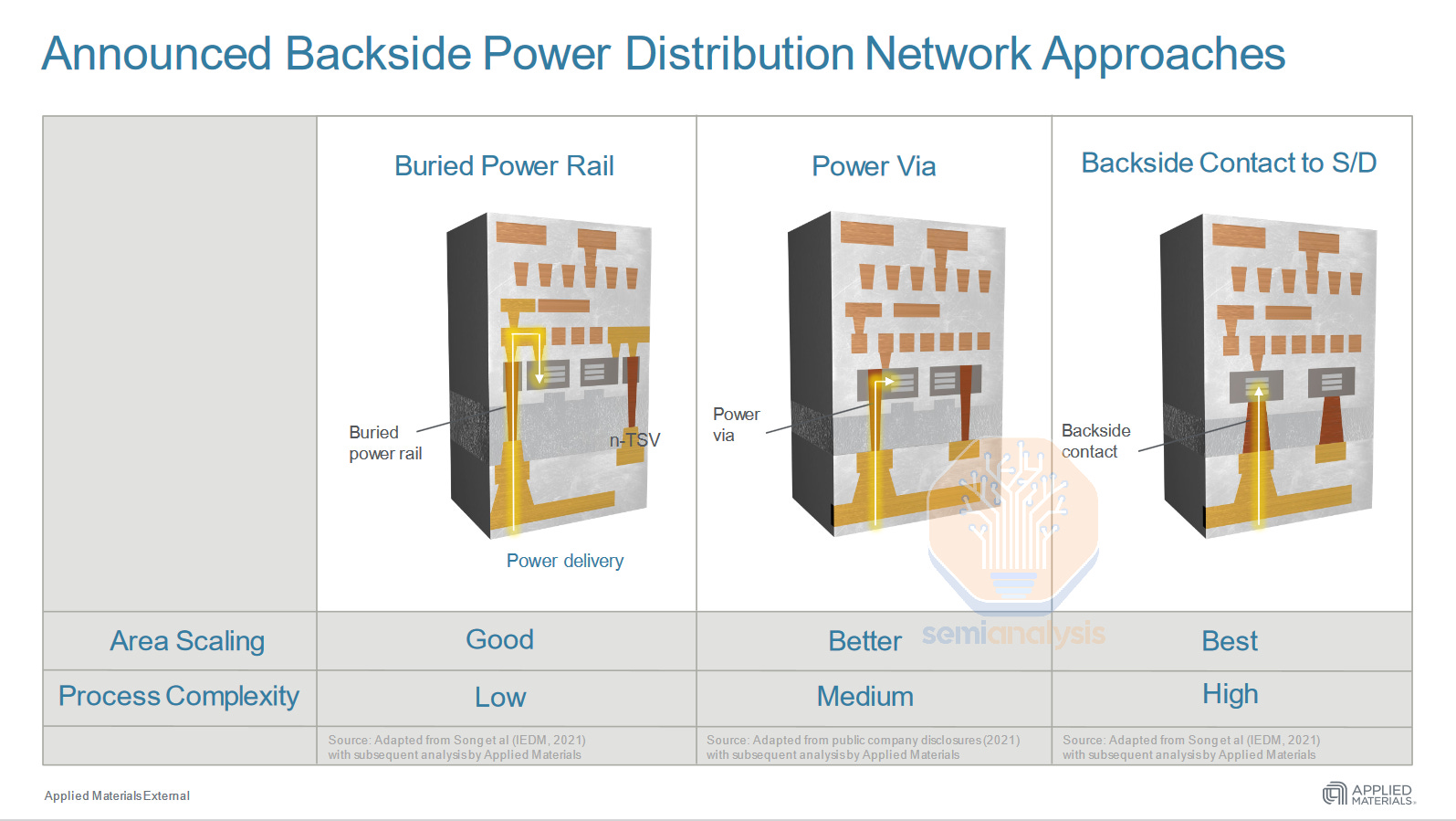
Buried power rail (BPR) is the simplest of the backside power implementations. Early research used this scheme and subsequent architectures built on this core idea. It entails moving the power rail from its normal location atop the transistors in the M2 metal layer, to its own level below the transistors. This enables an architectural shrink as the wide power rails are replaced by a thin, tall rail tucked closely beneath the transistors. However Buried power rail still connects to the transistors via a frontside metal layer, and to the power delivery network on the backside with through silicon vias (TSV). This means the overall cell height can be reduced by ~1T, or roughly 15%.
Constructing BPRs is relatively simple but has one major risk: using metal in the front-end-of-line (FEOL). Metal is traditionally limited to middle-of-line (MOL) and back-end-of-line (BEOL) processes, after the transistors have been fabricated. This is to avoid contaminating the semiconducting devices with conductive metal. Fabs are serious about this – many have FEOL-specific tools forbidden from running any wafers that have metal layers. Fabs must break this rule to construct buried power rails, as by definition BPRs must be integrated before the transistors. In reality nobody wants to break this rule, and it appears BPR will not be adopted in any HVM processes.
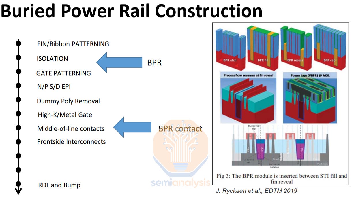
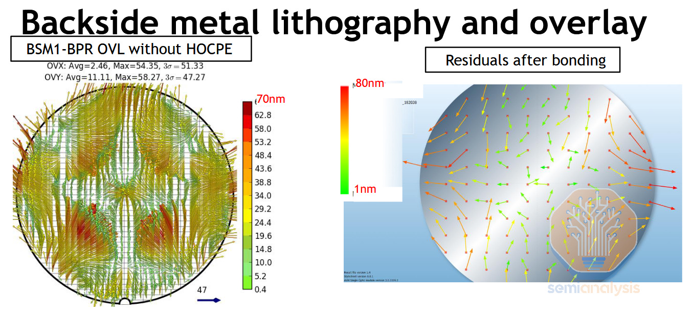
Aligning the initial backside features connecting to the buried rails is another challenge. Bonding onto the support wafer induces distortions that must be corrected, making post-bonding litho much more difficult. ASML and others have made remarkable progress here, and post-bonding overlay capabilities are good enough for BPR schemes – but at the edge of spec for more complex options like backside contacts.
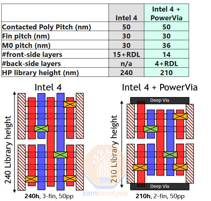
PowerVia is Intel’s backside power solution. It improves upon BPR in two major ways:
-
Power rails are moved to the wafer backside, avoiding contamination risk of BPR.
-
Better cell scaling as power routing is eliminated from the wafer frontside.
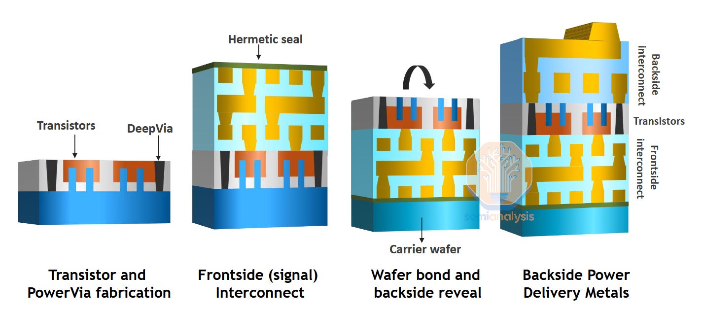
PowerVia is a clever evolution of the BPR concept. During front-end processing PowerVia skips the power rail entirely. Along with avoiding the contamination risk of depositing metal before the transistors, it also eliminates an expensive alignment-critical process step (aligning BPR to transistor channels). At giga-fab scale, a single critical layer like this can cost in the low hundreds of millions USD in tooling.
The only added step from a traditional all-front side scheme is the tall, skinny PowerVia constructed just after the transistor contacts. This via runs from the contact deep into the bulk wafer substrate. After completing the frontside, the wafer is flipped, bonded, and thinned. Because the vias extend deep into the wafer backside, they can be revealed during thinning without risking damage to the transistors. This clever “self-aligned” approach greatly simplifies the backside patterning that must align to the PowerVias (self-aligned in this contact really means the alignment requirements are greatly relaxed i.e. cheaper and better yielding).
This approach also has scaling benefits. BPR connects to the transistor with a via from the top of the transistor contact, through a metal layer on the front side, then through another via down to the BPR itself. These low metal layers are one of the key scaling limiters as they require some of the smallest features and very congested routing – by routing power through it, BPR does little to relieve the issues there. PowerVia helps. Routing straight from the transistor contact down to the BSPDN means there truly is no power routed through the critical frontside metal layers. This means the pitch of those layers can be relaxed (improves cost), scaling can be more aggressive, signal wires can take the place of the relocated power wires, or some mix of the three.
Yet there is still some standard cell scaling left on the table. The PowerVia, while thinner than a BPR, still contributes to the total cell height.
Direct backside contacts (DBC or BSC for BackSide Contact) offer a way to eliminate the contribution of power to standard cell height. In other words, they achieve the greatest scaling benefits of any backside power scheme. The idea is a natural extension of BPR and PowerVia- rather than route the power from the top or side of the contact, route it through the bottom.
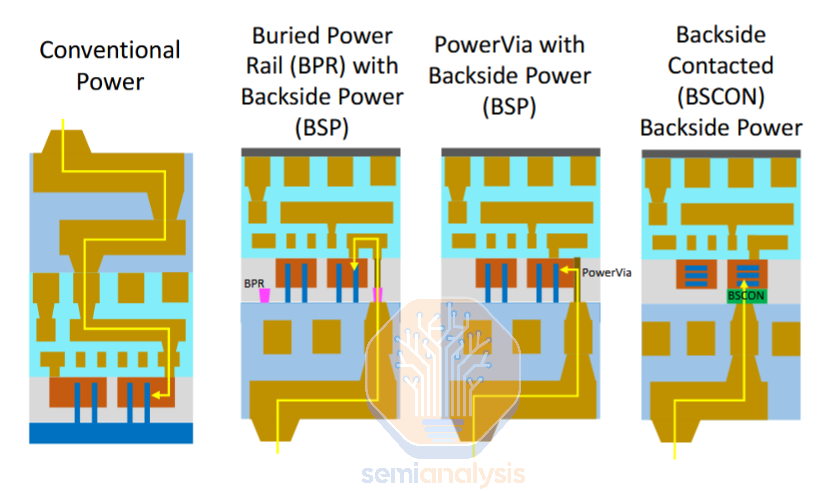
While the idea is simple, it turns out that backside contacts are the highest risk, highest reward BSPDN option. Manufacturing them is not easy. The main driver is the pitch, or how close together, the contacts must be aligned to other features. For BPR and PowerVia, the features connected to the backside are roughly the same pitch as the height of the cell, something like 150-250nm for a modern cutting-edge process. The overlay required in post-bonding lithography to pattern the first backside power layer is >10nm. This overlay and >150nm pitch is easily achievable by cheap(er) DUV scanners.
For direct backside contacts, the requirements are much more difficult. Contacts for power routing are formed beneath sources and drains. The source to drain distance is roughly equivalent to the contacted poly pitch (CPP), the distance from gate to gate. The CPP of modern processes is well known so it gives us a rough idea of the pitch required for the BS contacts – on the order of 50nm. This is well beyond the resolution of a single ArF immersion exposure, necessitating a more expensive multi patterning schemes or EUV. Overlay also becomes challenging as the spec is somewhere <5nm. Normally this is not a problem for high-end scanners but extremely challenging here due to the high-order distortions locked in by wafer bonding.
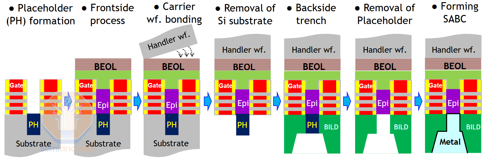
Another challenge is metal use in FEOL, but modern backside contact schemes have a clever workaround here. Like BPR, they require an additional feature fabricated before the transistors. But the contact is initially filled with a non-conductive placeholder material, not metal. Once the placeholders are revealed during thinning (like PowerVia, these features are self-aligned), they can be etched away and replaced with metal. This trick doesn’t work well with BPR as they are high aspect ratio, so it would be difficult to cleanly etch out a placeholder material.
Despite being difficult to produce, the benefits of backside contacts are substantial: a 6T frontside-only cell can theoretically be scaled down by roughly 25%, to 4.5T or even 4T. In practice rather than scale the cell, a signal wire can be routed in place of the relocated power rail. This significantly improves routing and at the chip level still achieves a density increase. Line resistance is significantly reduced with power savings ~15%. Clock frequencies can be increased by more than 5%. Reliability is improved as wires on both front and backside can be larger, reducing risk of electromigration and allowing for faster switching or higher currents. A study from IMEC, Google, and Cadence presented at VLSI this year found the greatest benefits realized in high power (HP) libraries, commonly used for HPC applications such as AI accelerators.


Note that these benefits are not free. Total layer counts increase by up to 20%. Wafer thinning, while not affecting active elements like transistors, can degrade the performance of passive devices such as diodes that depend on thick Si – workarounds will be needed. All backside processes must be compatible with frontend devices: namely, they must not require high temperatures that would ruin the transistors.
In the future, the backside will not be limited to just power and global clock. It is likely that signals and BEOL devices such as capacitors (Intel is already showing MIM capacitors in the backside redistribution layer) will also move. For stacked transistors (CFETs) this will be important, as the signal for the bottom device must be routed through backside to realize full scaling benefits. The 1.4nm nodes and beyond should start to include greater complexity on the backside.
There is a surprising amount of variation, in both timing and architecture, for GAA and BSPDN on the foundry roadmaps.
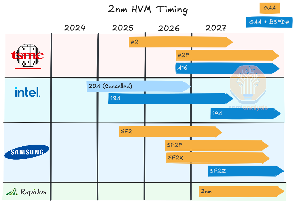
Starting with the latest entrant in the foundry race: Rapidus is a nascent Japanese foundry born from a desire to reclaim parity in advanced semiconductor manufacturing. They are heavily subsidized by the Japanese government with additional funding from 8 large domestic companies including Toyota, Sony, and others. Their stated ambition is to open a 2nm pilot line in April 2025 with high volume manufacturing in 2027 and further node development to at least a 1.4nm node. This is a brand-new company trying to go from incorporation in 2022 to high-volume manufacturing (HVM) at the bleeding edge of logic in 5 years. We believe it’s going to be very tough journey ahead of them.
Via a joint development partnership, Rapidus will license IBM’s 2nm process technology and put it into production. The process has not been used in high volume (IBM’s server chips were made on old GlobalFoundries nodes and now Samsung 5nm). The process emphasizes small batch sizes to enable fast iterations and fast learning. This might make sense for a nascent company trying to ramp leading edge logic but they are trading learning speed for high volume efficiency. There’s a reason why their competitors use large batches.


Small batch sizes enable faster processing times in certain steps such as bakes – where small chambers are easier to heat and cool. But they heavily increase the need for metrology. For a large batch it is common to do metrology on one wafer and assume similar results for the other 24+ wafers processed at the same time. Small batches effectively mean each wafer is a “special snowflake” that needs its own metrology. The added metrology burden should outweigh the advantages of small batches.
Their business proposition is also questionable. Where is their place in the market against the TSMC juggernaut, a process-competitive but financially challenged Intel, and Samsung, which can muster the focus and financial resources of its entire chaebol (and country)? What would motivate a customer to move IP onto a new process that is planned for just 25k wafer starts per month of capacity (versus a typical 100k+ for TSMC in the first few years of HVM)? There is little to no domestic demand in 2nm logic for the Japanese government to push towards Rapidus. It is difficult to see how they will find a competitive advantage in performance or cost. So far no clients with meaningful volume are signed up – Tenstorrent is confirmed and IBM is likely to test it for its mainframe chips.
Additionally, their roadmap does not include backside power delivery. This will be a disadvantage in HPC applications where competing processes will offer better performance and density by including BSPDN. R&D on single wafer batch tools doesn’t easily transfer to that on multi-wafer batch tools
Samsung is also “customer challenged” but pushing ahead with an ambitious roadmap. They were technically the first to mass produce GAA back in 2022 at the SF3E node, but this was not productized in any meaningful way. SF2 is therefore more of an evolutionary node rather than revolutionary. It’s likely that one of Samsung’s upcoming nodes will add a 4th nanosheet to the stack – most others are using 3 for the foreseeable future. SF2P will offer higher speeds with slightly lower density than SF2.
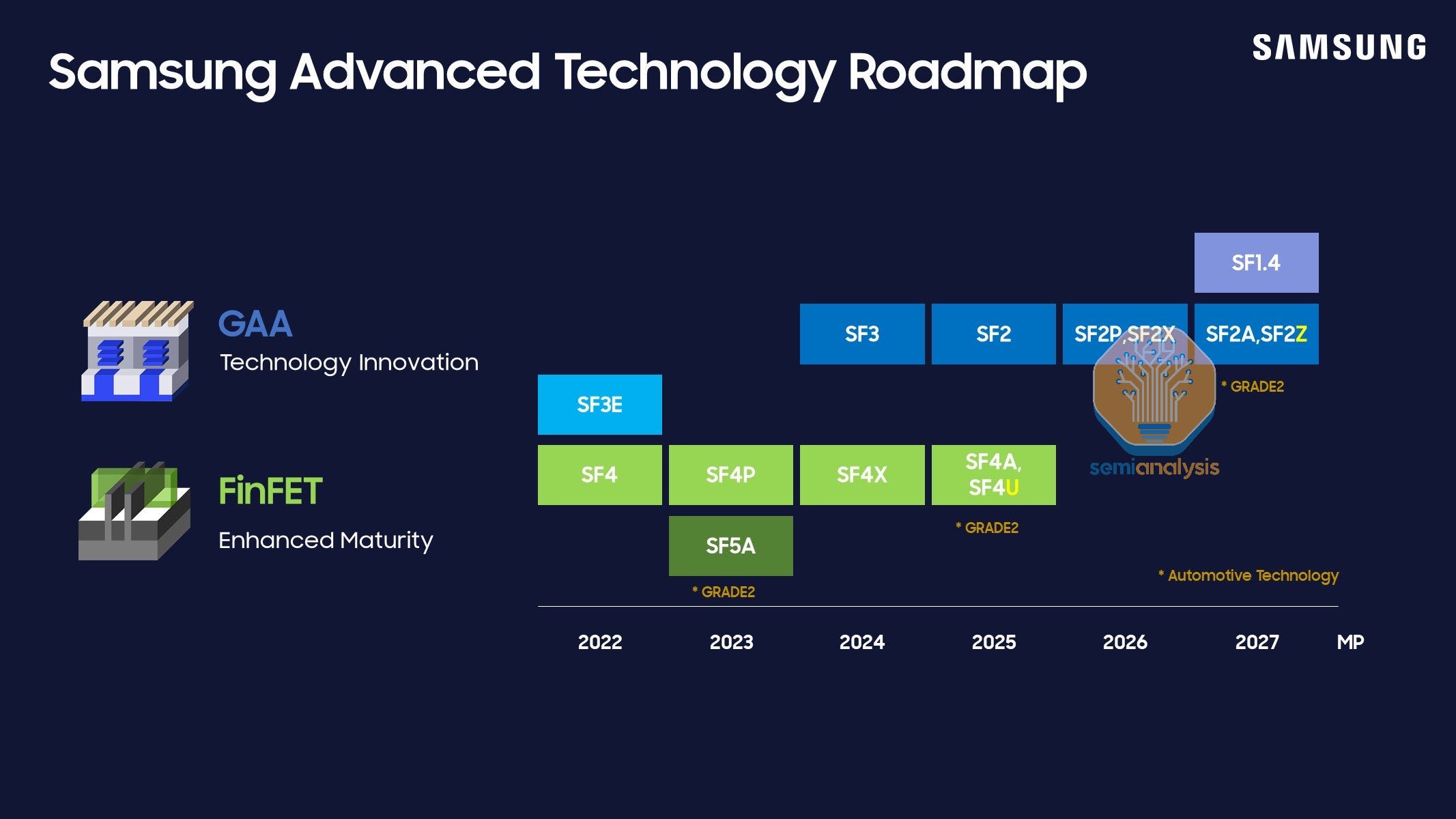
The main highlight on their roadmap is the introduction of backside power in 2027 at the SF2Z node. Detailed at the Samsung Foundry Forum in June 2024, the process will implement backside contacts to move power and global clock to the backside. Performance increase is stated at 8% along with 15% reduction in power and 7% in area – all relatively reasonable claims.
SF1.4 will scale both metal and gate pitches and involve some sort of change to the nanosheets that was only teased. Possibly it could be 2D channel materials although this would be extremely aggressive timing.
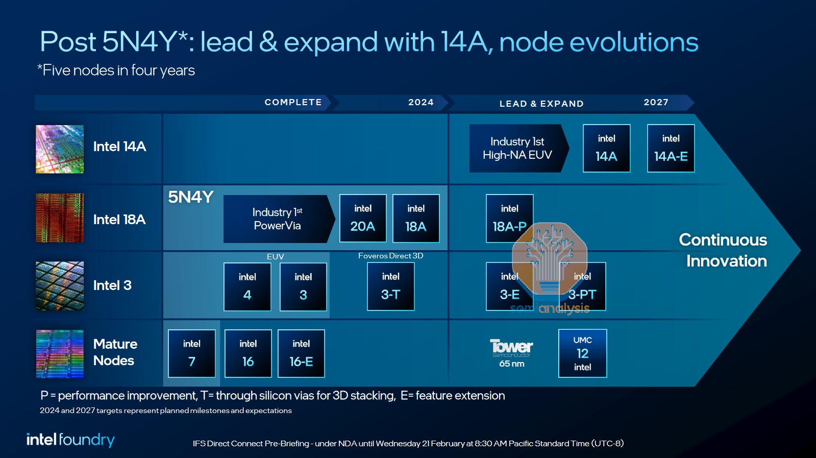
Intel is already ramping its GAA + BSPDN node, 18A. The preceding 20A process was recently abandoned but for financial reasons, not technical. With the recent report that 18A defect density is on-track, it appears the process tech is maybe the one thing going well at the company right now.
We’ve discussed Intel’s roadmap and foundry prospects in much greater detail:

Notably, Intel is using a PowerVia scheme for backside power. As we detailed above, this should be slightly easier to fabricate but offer less scaling benefit relative to direct backside contacts.

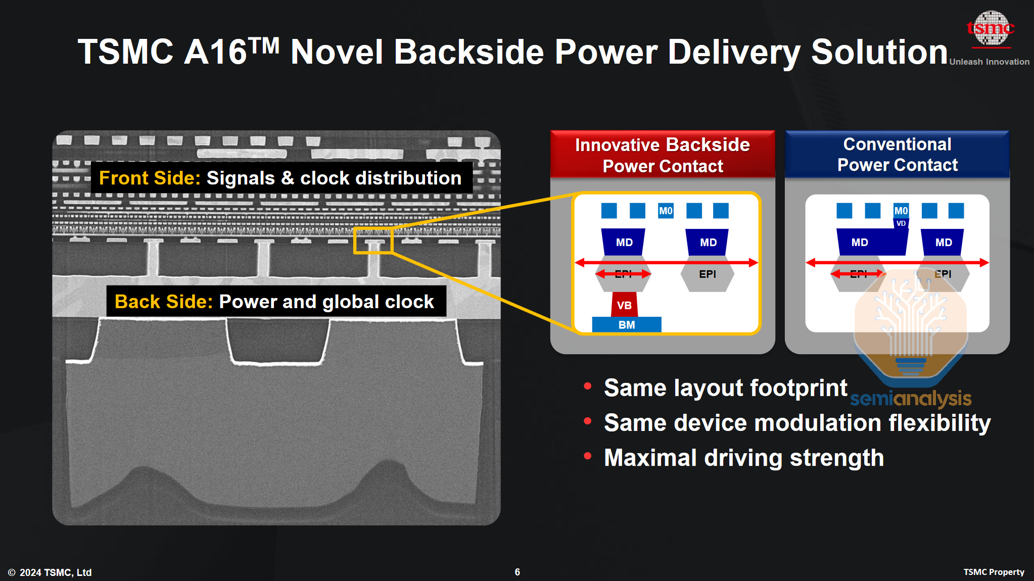
With N2, TSMC continues its steady drumbeat of process node improvements that have driven its share price to continue compounding years of gains. N2 is ramping to high volume next year with TSMC’s first GAA architecture but without BSPDN. Variants N2P and N2X offer mild improvements in 2026 along with the first GAA + backside power node, A16, in the 2nd half of the year. Like Samsung they are choosing to dive headfirst into BSPDN with a backside contact scheme rather than the easier, more conservative BPR or PowerVia options.
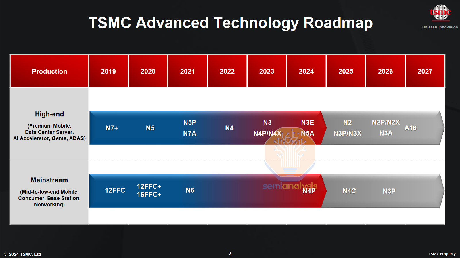
Their implementation of backside contacts appears to be conservative in its 1st generation. A claimed 7-10% density increase is roughly half of what’s possible from cell scaling in theory. This is probably done to maintain design compatibility with N2, likely the FEOL will stay the same and only routing must be redone to utilize the backside power network. IR drop is also significantly reduced with up to 20% power improvement possible.
Each foundry’s implementation of GAA is broadly similar, the differentiator being how aggressive they are in feature scaling. Their claims for performance, power, and density vary widely – these should be taken with a grain of salt until independently verified.
SRAM scaling is a key driver for improving chip capabilities generation-on-generation, as it’s the fastest memory and closest to logic. Every chip designer wants more SRAM (without compromising in chip area or cost). Yet SRAM bit cell scaling has stagnated since the 5nm node with TSMC’s N3 and N2 nodes offering little to no bitcell scaling. Most of the scaling strategies that enabled shrink elsewhere either aren’t useful or were implemented long ago in SRAM cells. For example, single-fin transistors were finally offered for logic at N3 – but high density SRAM has been single-fin since Intel 22nm, the 1st finFET process. Backside power offers little benefit as bit cell routing is already optimized.
Transistor length and width reduction is the strongest lever for SRAM bit cell scaling. Compared to a single-fin device, a GAA transistor is slightly smaller since the transistor channel length and spacing between transistors can be reduced. This means the bit cells will see a one-time scaling benefit in the change from finFET to GAA, but likely not much in follow-on nodes.
Contacts, connecting transistors in the bit cell to power and signal, also restrict cell scaling. They must be large enough to form a low-resistance connection and maintain a minimum separation to avoid shorting between adjacent contacts. These are scaling slowly as well with advances in material engineering.
SRAM periphery, like other logic, still benefits from modern DTCO (design technology co-optimization) and other scaling techniques. When TSMC claims as 22% SRAM density improvement from N3E to N2, it comes mostly from periphery scaling. Unfortunately, in key applications such as working memory and L2 or L3 caches, periphery is only a small percentage of the total SRAM area and thus the benefits will not be as strong here. Overall performance improvements, if they meet claims, will come primarily from logic cells, not SRAM.
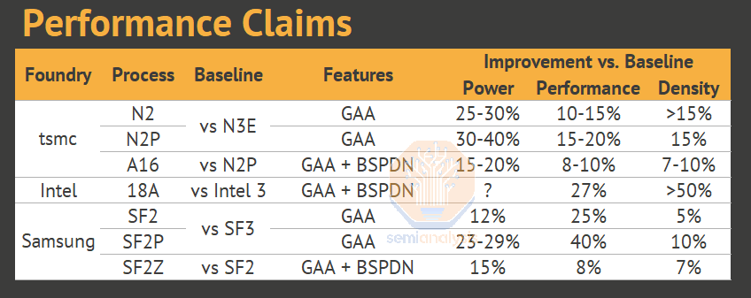
The real high-volume introduction of GAA will be 2025 for all three large foundries, with Rapidus following in 2027. Intel will be first by a year or so with BSPDN, but at a density closer to 3 nm processes despite the name 18A.
Next we’ll detail the cost of building 2nm fab capacity and the changes downstream to wafer fab equipment, including which companies stand to gain in the next decade of GAA nodes.