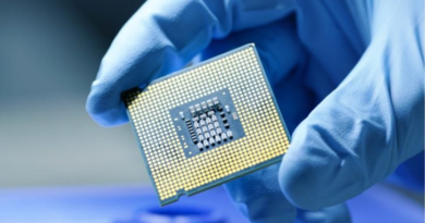
TSMC adopts 3D stacking tech for chips along with Google and AMD – Industry Leaders Magazine
Taiwan Semiconductor Manufacturing Co. (TSMC) the world’s biggest chip-making contract company has found a new way to manufacture chips along with Advanced Micro Devices or AMD and Google.
In a bid to find innovative ways to pack more information on a tiny chip, the semiconductor maker has come up with a new way of packaging more in a tiny space.
Chip packaging is a part of the final stage of the process of chip making. Semiconductors are placed in another case before being put on a printed circuit board.
TSMC is now using a new 3D technology called SoIC to stack and link several different types of chips — such as processors, memory and sensors — into one package, according to the company.
The SoIC method makes the chips more efficient and powerful.
These new 3D technology chipsets will be manufactured at TSMC’s new factory in Miaoli in Taiwan. The plant will be built by 2021 and the mass production for the chip will begin at latest by 2022. Google and AMD have already committed to the SoIC chips and are helping TSMC to test and certify them.
TSMC supplies chips to Apple, Qualcomm, Nvidia and Broadcom, almost all the big players in the market. Earlier, it outsourced the chip packaging part to specialized suppliers, including ASE Technology Holding, Amkor and Powertech, Chinese companies such as Jiangsu Changjiang Electronics Technology, Tongfu Microelectronics, and Tianshui Huatian Technology Co.
But the SoIC technology will enable TSMC to complete the whole chip-making process under its own steam. “TSMC is, of course, not trying to replace all traditional chip packaging players, but it aims to serve those premium clients at the very top of the pyramid so those deep-pocketed chip developers like Apple, Google, AMD and Nvidia won’t leave TSMC for its competitors,” said a person in the know to Nikkei Asia.
“These new chip stacking techs require advanced chip manufacturing expertise as well as a lot of computer simulations to achieve precise stacking, so it’s very difficult for traditional chip packaging providers to step in,” said another chip packaging industry expert.
There are other players in the market who are also experimenting with chip packaging. Semiconductor Manufacturing International Co, (SMIC) China’s biggest contract chipmaker, is already exploring possibilities of manufacturing chips using the 3D stacking method and has tapped the suppliers that supply equipment to TSMC.
It will be certainly difficult for the Chinese SMIC to compete with TSMC, especially due to the US government’s increased restrictions on trading with Chinese companies and the use of any technology developed by US companies.
“Still, we clearly see SMIC’s ambition to expand its footprint at the forefront of chip packaging, although it will take a lot of time,” one of the sources said.
Other semiconductor manufacturing giants—Intel and Samsung—are also betting big on next-generation chip stacking technology. Intel is building new generation chips with advanced packaging capabilities for in-house consumption mainly.
Samsung is expanding its factory output and will be supplying to Qualcomm and Nvidia, its key customers.
“We expect revenue from our back-end services, which include both advanced packaging and testing, to grow at a rate slightly above the corporate average in the next few years,” CC Wei, TSMC chief executive and vice-chairman, said in an earnings briefing in mid-October.
The SoIC based chips will be used by Google for its autonomous driving systems and other applications, a source said. Google too is making its own chips of use in its data center servers. AMD, which develops microprocessors for computers and servers, is also hopeful that the SoIC packaging method will boost its performance compared to its rival Intel.
TSMC, talking about its production method, said in a media interview that “it is necessary for semiconductor and packaging technologies to evolve together as customer demand for advanced chip packaging services is increasing.”
TSMC’s foray into chipmaking started in 2016 when it started supplying highly advanced chips packaged with processors for Apple’s iPhones.
Up until this year, most of TSMC’s chip packing revenue has been from Apple, according to Mark Li, an analyst with Bernstein Research.
Arisa Liu, a semiconductor analyst with the Taiwan Institute of Economic Research, said chip developers are seeking more advanced chips that pack more energy and performance together. “It has become a new arena for leading chip manufacturers TSMC, Samsung and Intel, as well as for global leading chip developers,” Liu said. “It’s also viewed as a means to counter the slowing of Moore’s Law.”
TSMC’s revenue from chip packaging and testing services reached $2.8bn in 2019, about 8 percent of its total revenue of $34.63bn, and is expected to grow at close to the same rate as its revenue for 2020, the company said.
The chip packaging industry was worth $29bn in 2019 and is expected to grow at a compound annual growth rate of 6.6 percent between 2019 and 2025, to reach $42bn in 2025, according to research agency Yole Development.
Your email address will not be published.
0%
