Giảm điện dung Transistor tại nút 5nm bằng cách sử dụng một rãnh tiếp xúc nguồn/cống
In logic devices such as FinFETs (field-effect transistors), metal gate parasitic capacitance can negatively impact electrical performance. One potential way to reduce this parasitic capacitance is to add a source/drain contact (CT) recess step when building the source/drain metal structure. However, this additional structure can potentially increase the source/drain to via resistance.
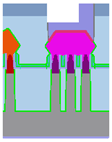
Using a 5nm logic test case, we investigated the impact of adding a source/drain contact (CT) recess step in the source/drain metal structure as shown in figure 1.
Fig. 1: View along the y-direction of model of recessed CT.
The purpose of this study was to determine whether adding a CT recess step could reduce the source/drain to metal gate (MG) capacitance without substantially increasing the source/drain to via series resistance. We will now review the results of using SEMulator3D virtual DOEs (Design of Experiments) to predict resistance and capacitance when adding a source/drain contact (CT) recess step.
Methodology
We trained a process model using a transmission electron microscopy (TEM) image. Once we built our model, SEMulator3D virtual fabrication and Design of Experiments were used to vary the recess depth and critical dimension (CD) to calculate the expected source/drain to via series resistance and the source/drain to metal gate capacitance.
For this methodology, we used the layout shown in figure 2.
Fig. 2: Layout showing the fins (blue), gates (green), regular source/drain contact (yellow), via (purple), N-well/P-well (red) bounding box (white) and the new source/drain contact recess mask (cyan).
Our original layout used a cell area focused on the PMOS field effect transistor (PFET) logic fins. We have seven fins, three gates, a via contact and two source/drain contact masks. We drew in a separate source/drain contact mask that was small (compared to the original source/drain contact masks) to introduce the recess. Next, we added an extra set of process steps to create the source/drain contact recess (see figure 3). The process sequence contained four extra steps. In our model, we assumed that there were no spacer pulldowns, and we assumed that a new CT recess etch was selective to only metals (to avoid having oxides etched during the process step).
Fig. 3: Extra process sequence for introducing the source/drain contact recess etch. Left hand side shows the cross-section view along the fin (x-cut). Right hand side shows cross section view along the gate (y-cut).
After building our 3D model, we completed two measurements: a via to source/drain resistance extraction, and a source/drain to metal gate capacitance extraction measurement. For the resistance extraction, we created ports at the source/drain PFET top and at the via top. The location of the ports is highlighted in blue as shown in figure 4. For the capacitance extraction, we assigned our nets to the recessed source/drain contact (CT) on the left-hand side of the metal gate, along with the regular CT on the right-hand side of the metal gate and the metal gate itself. For this study, we focused on the capacitance between the metal gate and the left S/D contact that was recessed as shown in figure 5.
Fig. 4: Named ports (blue) along PFET source/drain and the via top for resistance extraction.
Fig. 5: Named nets of left source/drain recessed contact (Recess_CT_L) and metal gate (MG) for capacitance extraction.
Next, we performed a full factorial DOE by varying 2 parameters (the CT recess depth and the CT recess Y bias) and measured the resistance and capacitance. The CT recess depth was varied from 0 to 55nm in 5nm increments and the CT recess Y bias was varied between 0 to 23nm/edge (only 23nm in the CT metal structure since we are only etching metals). We used twelve different values for the recess depth and twenty-four different values for the Y bias, for a total of 288 combinations of values and simulation runs.
Results
Looking at the resistance, the CT recess depth has a small impact on resistance (~+5% increase), while the CT recess critical dimension size in the y-direction has a significant impact on resistance (+304%) (see figure 6a). This is because the oxide fill affects the recess CT and creates a larger CT critical dimension in the y-direction. The oxide encroaches on the via bottom, which in turn affects the via resistance. This occurs because we are removing more of the CT metal that is under the bottom of the via. As the CT critical dimension in the y-direction increases, the area of cobalt (Co) contact metal and via bottom metal decreases, increasing the via resistance (figure 6b).
Fig. 6: a) Resistance contour plot of CT Recess Depth vs Recess CT Y Bias b) Resistance on left y axis and IF area on right y axis vs Recess CT Y bias.
Reviewing the capacitance, CT recess depth changes impact the capacitance. In our DOE, we saw a 20% decrease in MG to Recess CT L capacitance (figure 7a). The capacitance does not change much as we increase the recess depth. However, we do see a capacitance drop once the CT recess depth exceeds the delta from the CT top to the metal gate top (figure 7b). The CT Y bias, on the other hand, has a small impact on capacitance (only about a 4% decrease over the variation range).
Fig. 7: a) Capacitance contour plot of CT Recess Depth vs Recess CT Y Bias b) Capacitance between left source/drain contact to metal gate vs CT Recess Y bias.
Conclusion
In summary, we set up a methodology to introduce a new mask for a recessed CT and determined how it changed the metal gate resistance and capacitance. The CT recess depth has an impact on capacitance if the CT recess depth is larger than the delta of the CT top to metal gate top. However, it has no impact on resistance. The CT critical dimension in the y-direction has a significant impact on resistance as it decreases the interface area of the CT metal and the via bottom metal, which in turn increases the via resistance. For this study, we can decrease the source/drain to metal gate capacitance by making sure the CT recess depth is below the metal gate height while still maintaining the same source/drain to via series resistance. We can only do this if the CT critical dimension in the y-direction does not increase, impede the via bottom interface area and increase the resistance. From our study, we conclude that adding a CT recess step can reduce the source/drain to metal gate (MG) capacitance without substantially increasing the source/drain to via series resistance.
Pradeep Nanja
Pradeep Nanja is a software applications engineer at Coventor Inc., a Lam Research Company. He works with customers on process development, integration and yield improvement applications. Prior to joining Coventor, he worked at GlobalFoundries, driving process deck development for GlobalFoundries 7nm technology. In this position, he helped identify downstream foundry process issues using techniques such as process window analysis and cross wafer analysis. Nanja received his B.S. and M.S. degrees in Materials Science and Engineering from UCLA.


