Calibre DesignEnhancer cải thiện quản lý năng lượng nhanh hơn và sớm hơn

Anyone who has attempted to implement a custom design in an advanced process node knows that effective power management can be quite challenging. Effects such as voltage (IR) drop and electromigration (EM) can present significant headaches for both design teams and foundries. Optimizing layouts for these kinds of issues is tricky. Design and P&R tools are intended for optimal design creation and implementation. Layout optimization can be an afterthought. Design for manufacturing (DFM) layout tools are good at optimization, but they are used at signoff, and the goal is to use it earlier in the design flow. There is a technical paper from Siemens Digital Industries Software that details an effective solution to this dilemma. A link is coming, but let’s first examine some details to see how Calibre DesignEnhancer improves power management faster and earlier.
About the Publication and the Author

The paper from Siemens is entitled Calibre DesignEnhancer Design-Stage Layout Modification Improves Power Management Faster and Earlier. The author is Jeff Wilson, a product management director for DFM applications in the Calibre organization at Siemens Digital Industries Software.
Jeff is responsible for the development of products that analyze and modify IC layouts to improve the robustness and quality of the design. Before joining Siemens, he worked at Motorola and SCS. He holds a B.Sc. in design engineering from Brigham Young University and an MBA from the University of Oregon.
Jeff has quite a passion for layout optimization, and it comes through clearly in this well organized and insightful technical paper. You can see a short video of Jeff providing an overview of Calibre DesignEnhancer. A link to that is coming as well.
The Problem
At advanced process nodes, the challenge of managing capacitance and resistance impacts rises sharply. For example, going from 16nm to 5nm we see a max resistance increase around 6X. Over-designing the power grid results in wasted area. Under- designing can result in the IC never achieving IR and EM requirements. What is needed is a solution where the power grid is designed to be efficient for most of the design and optimized for areas of the layout that must support greater power usage.
Custom/analog designers and design implementation engineers have all the physical details needed for accurate and efficient layout optimization. However, applying layout modifications during design and implementation has typically been difficult and/or time-consuming. As discussed, most design and P&R tools provide native options that allow engineers to apply some layout optimization changes to layouts, but custom design and P&R tools are designed and intended for design creation and implementation. The result is sub-optimal layout optimization.
Some of the specific challenges to be met here include IR drop and electromigration. For the first item, the overall size of the chip may be similar at advanced nodes, but the transistors and interconnect are packed into a smaller area. Typically, that results in the interconnect becoming narrower, which increases the unintended (parasitic) resistance, causing the voltage of the current traveling through that interconnect path to decrease over the length of the path (IR drop).
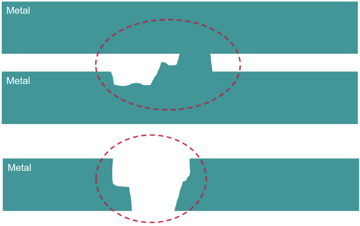
For the second item, metal atoms can be “pushed” out of place by the flow of current through the interconnect. Over time, the movement of these metal atoms creates both empty spaces (voids) and piles of atoms (hillocks) in the interconnect. If the voids become wide and/or deep enough, they create an open circuit in the interconnect, while hillocks can grow high enough to connect to other interconnects, creating a short. This is a ticking time bomb in advanced circuits that needs to be handled carefully. The figure below illustrates what can happen.

The Solution – Design Stage Layout Modification
To ensure a design remains compliant with design rule checking (DRC) constraints, all layout modifications must be applied with a deep understanding of complex design rules and connectivity requirements. The Calibre DesignEnhancer tool provides an analysis-based solution integrated with both design and P&R flows to help custom designers and P&R engineers efficiently and accurately reduce IR drop and EM issues without negatively impacting performance and area. The tool is used early in the design process, creating a Shift-Left solution that optimizes results and avoids long design/analysis loops.
This approach prepares layouts for physical verification more quickly with minimal issues encountered. Multiple automated layout enhancement use models accessing proven, foundry- preferred rule decks provide optimized layout modifications while ensuring all layout changes are Calibre-clean. The technical paper goes into significant detail about the challenges in advanced designs and how Calibre DesignEnhancer addresses those challenges. If advanced node design is in your future, you need to download this technical paper to improve your chances of success
A download link is coming. First, I will summarize the solutions presented in the paper.
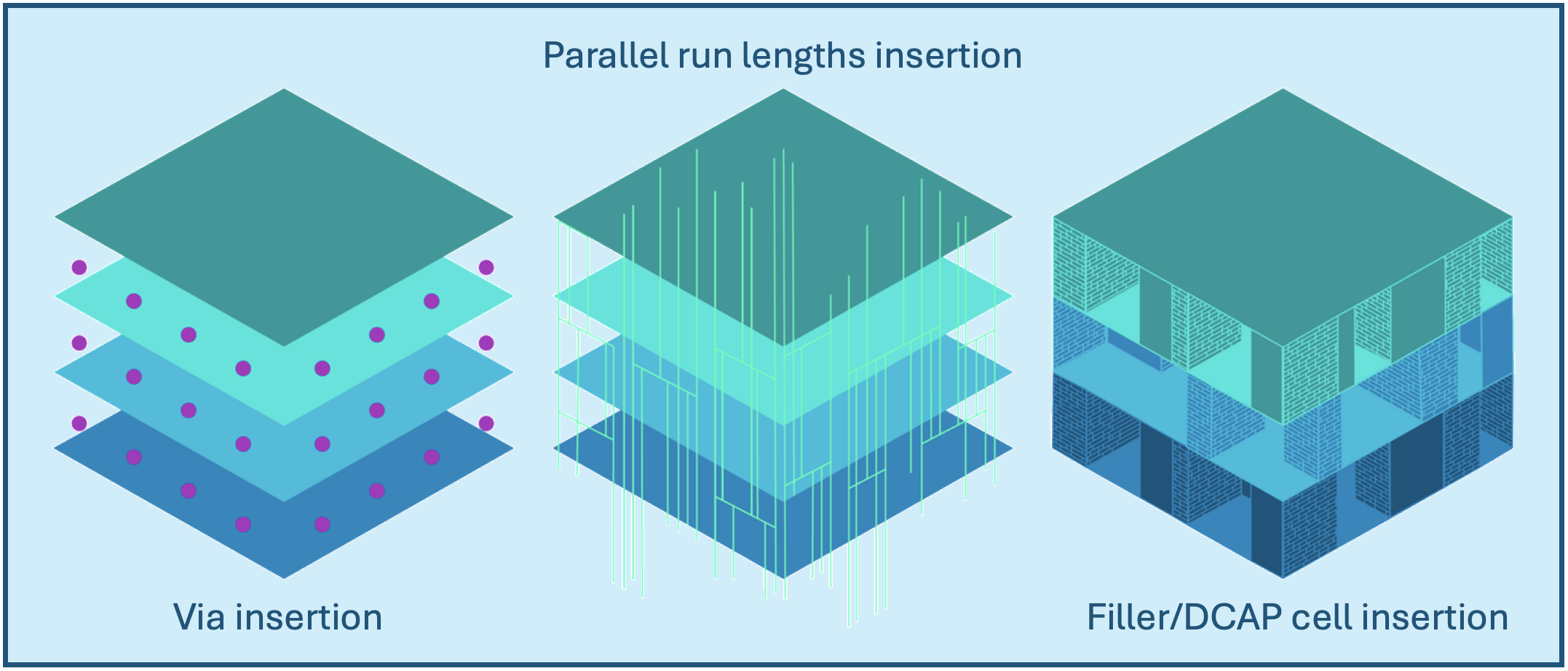
The Calibre DesignEnhancer tool currently provides three use models:
Via insertion, that automatically adds Calibre-clean vias to reduce IR drop and moderate the impact of via resistance on manufacturability and reliability.
Parallel run lengths insertion with the power grid enhancement (Pge) use model that automatically reduces resistance by finding open tracks and inserting Calibre-clean metal and vias to create these parallel runs.
Filler/DCAP cell insertion. In this case, open areas that are left between cells after P&R must be filled before physical verification can be run. These gaps are filled with filler cells (non-functional cells used to continue the rails as required for layer continuity and alignment, such as power/ground and Pwell/Nwell) and DCAP cells (temporary capacitors added between power and round rails to counter functional failures due to IR drop).
By replacing time-consuming and limited P&R filler cell insertion processes with the push-button Calibre DesignEnhancer Pvr use model and its knowledge of Vt rules, design teams can ensure not only Calibre-clean filler and DCAP cells, but also electrically-correct layouts, while also reducing filler cell and DCAP cell insertion runtimes.
These three use models are the inspiration for the graphic at the top of this post. The paper also details the design flow, compatibility with commercial tools and presents several detailed results.
To Learn More
Now it’s time to get your copy of this technical paper and prepare for your next advanced node design. You can download the paper here. And if you have a couple of minutes you can watch a great overview video presented by Jeff Wilson at the top of this page. And that’s how Calibre DesignEnhancer improves power management faster and earlier.
Share this post via:


