Nhìn kỹ hơn vào việc khắc phục hiện tượng rung đồng hồ với Infinisim
As voltages go down and frequencies increase, the challenges in chip design become increasingly complex and unforgiving. Issues that once seemed manageable now escalate, while new obstacles emerge, demanding our attention. Among these challenges, clock jitter stands out as a formidable threat. At its core, clock jitter is defined as the variation of a clock signal from its ideal position in time. Seemingly minor, these kind of subtle variations in the clock can cause catastrophic failures in high-performance designs. Previously, Dan Nenni provided a great overview of the problem and what Infinisim is doing about it here. Recently, I had the opportunity of speaking directly with the co-founder of Infinisim, where I gained profound insights into the enormity of the clock jitter problem and the monumental efforts required to address it. Read on for a closer look at conquering clock jitter with Infinisim.
Contributors to Clock Jitter
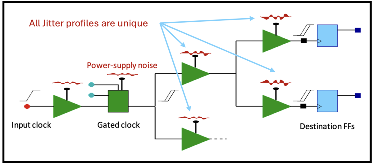
There are two main contributors to clock jitter – the PLL and the power delivery network (PDN). The PLL can deliver a noisy input signal to the clock circuit, creating jitter in the clock. In this case, the jitter is the same throughout the entire clock since it comes from one source. This localized effect isn’t the main focus for Infinisim’s tools. Instead, the company focuses on a much larger and more complex system design challenge, PDN induced jitter.
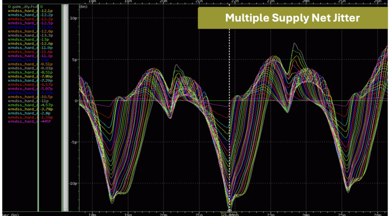
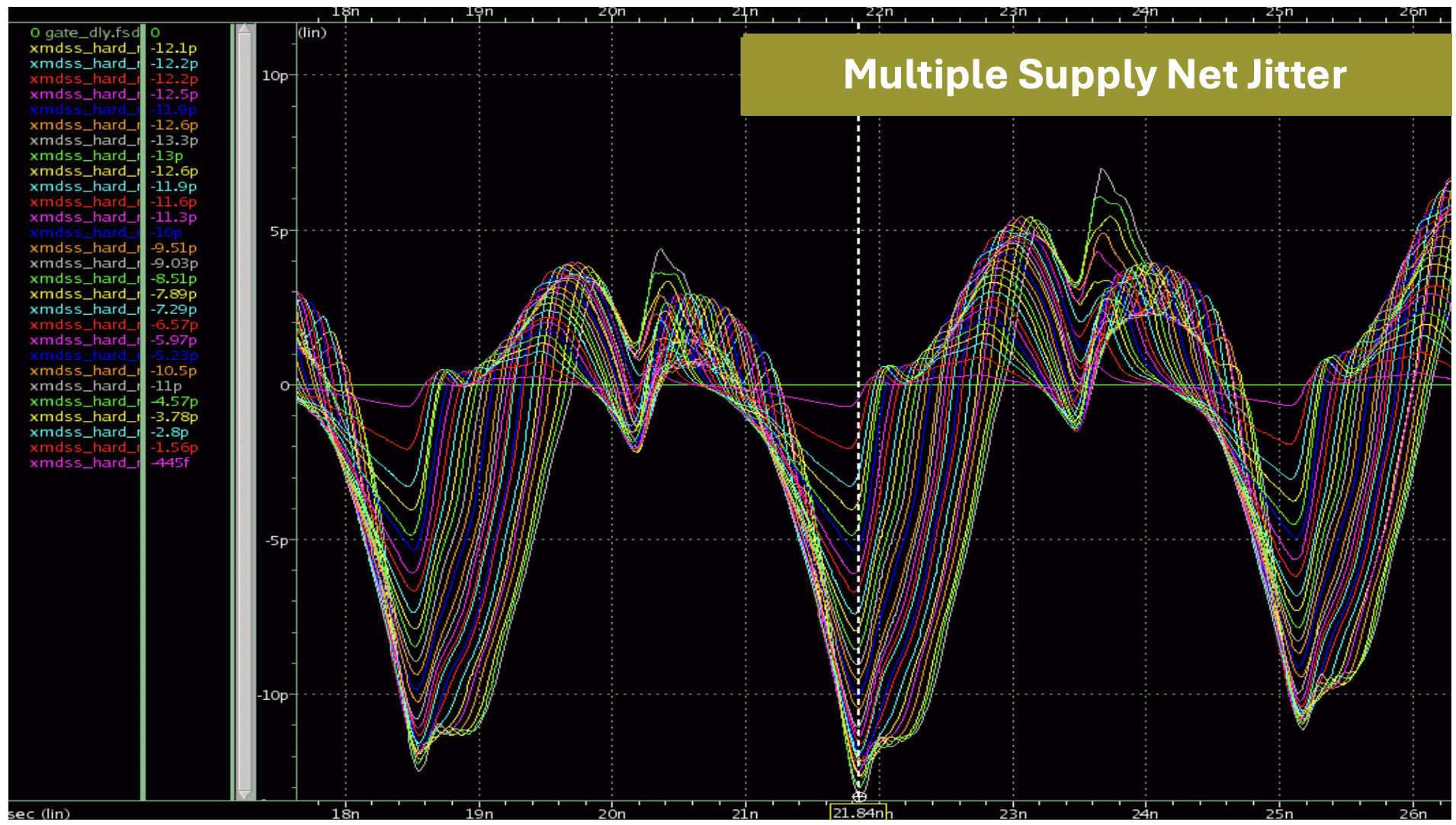
PDN jitter arises from a noisy supply voltage. Unlike PLL-induced jitter, PDNs can be influenced by multiple input pins and encompass numerous power domains. Add to that the local effects at each gate and you begin to see a pervasive and difficult to track problem. This is the area where Infinisim concentrates its efforts. The figure below illustrates these challenges.
What it Takes to Fix Clock Jitter

I had a highly informative discussion with Dr. Zakir Hussain Syed. Zakir is a co-founder and CTO at Infinisim with over 25 years of experience in EDA. His deep understanding of the issues was evident throughout our discussion, and I gained a wealth of knowledge from our exchange.
Zakir began by explaining the components of PDN-induced clock jitter. In the case of the PDN, every gate in the clock can see some level of noise-induced jitter. Each is an independent event, and the movement of clock edges is very small. Each event has the potential to change timing and behavior of the circuit. To find the best- and worst-case jitter in the circuit requires simulation of thousands of clock cycles – the errors can compound and the only way to find that is to simulate many cycles.
Furthermore, since the edge movement is very small, the simulation must be highly accurate. So, finding PDN-induced clock jitter requires SPICE-level accurate simulation over many cycles as quickly as possible. Remember, this is part of the verification loop, so speed is quite important. Do you have a headache yet? I began to at this point.
As Zakir continued, the problem got worse. Clock domains are becoming more complex thanks to multiple voltage domains. This creates more independent noise sources. Beyond that, power comes into the chip through many bump connections – potentially hundreds of bumps. Each bump will have its own noise signature which yet again increases the variety of issues that must be analyzed.
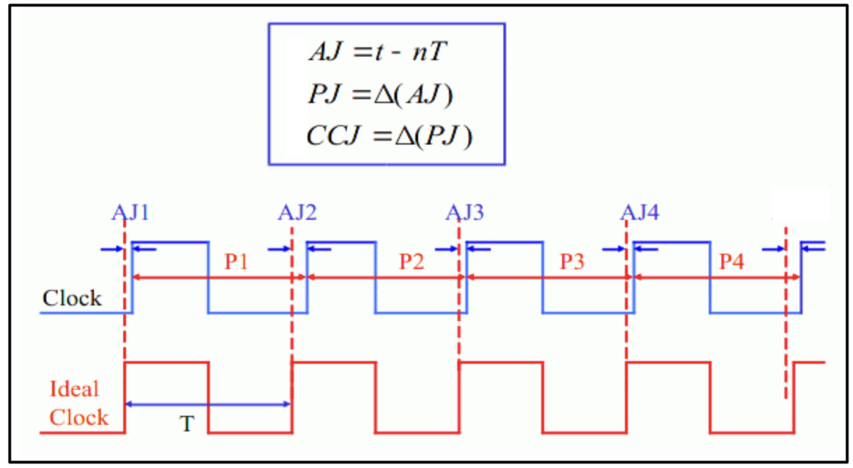
All this creates multiple types of clock jitter:
- Absolute jitter:
- The actual transition time compared to the ideal clock transition time
- Period jitter:
- The difference between actual transition and ideal transition at each period
- Cycle-to-cycle jitter:
- The difference in period jitter between two adjacent cycles periods
The figure below summarizes these effects.
Zakir then provided a bit of history for perspective. For the case of on-chip variation (OCV), initially the worst-case number was used for guard banding. As designs got more complex, applying just one number created an overly pessimistic metric and the result was very poor circuit performance. For many years now, OCV is calculated across the chip at a very fine-grained local level to provide more realistic guard bands. We are now at a point where the same strategy needs to be applied to clock jitter guard banding. A single number must be replaced by fine-grained analysis across the entire clock of the chip.
That fine-grained analysis looks at the noise per gate, per path, per noise profile for each cycle. Designers are looking for the best and worst-case jitter on a local level to develop the guard banding to use. It turns out the worst-case jitter can happen anywhere in the path, not just on the input of the flops. If you couple that fact with the per noise profile analysis, designers cannot only develop much more accurate guard bands, the jitter in the circuit can also be reduced.
Zakir explained that the per gate analysis can identify the weakest gate in the path from a jitter perspective. That gate can then be modified to be less susceptible to jitter. The per noise profile analysis can find the power bumps that generate the most noise and those, too can be modified to improve performance. All this helps improve the overall circuit performance in meaningful ways.
So, how does Infinisim manage to analyze all those profiles, circuits and scenarios over thousands of cycles with sub-picosecond resolution in a reasonable time frame? Zakir explained that relying on traditional SPICE simulations isn’t feasible – it will simply take far too long. Instead, he detailed Infinisim’s holistic approach to tackling this challenge.
First, the noise in the circuit is developed either with a commercial IR drop tool or with measurements if the silicon is available. That data is then analyzed by Infinisim’s ClockEdge and JitterEdge tools holistically across full clock domains. Using this analysis of the data over many scenarios finds the positive and negative jitter at every gate in the clock.
What is the Impact of Clock Jitter?
Just how big a problem is clock jitter? Consider there are several potential impacts on chip performance and reliability. These include:
Slower chip performance: Clock jitter leads to timing uncertainties. This can cause data to arrive too early or too late, resulting in timing violations. To mitigate this, timing margins are increased which slows the clock frequency.
Lower yield: Clock jitter can cause a higher rate of timing failures, particularly in chips operating close to their performance limits. This can lead to a higher percentage of chips failing during testing and thus a lower manufacturing yield.
So, the question is, what’s the impact of the above effects? Here is one quick “back of the envelope” calculation. Assume a manufacturing cost per chip of $50 for a design with a projected volume of 1 million units. Further assume an expected yield without jitter issues of 95%. If we assume that jitter lowers yield by 5% (a 5% drop in yield due to jitter is a reasonable assumption for a high-volume production environment where even small timing issues can have significant impacts), the following will result:
- Design without jitter issues:
- Chips produced: 1,000,000
- Yield: 95%
- Good chips: 950,000
- Cost per good chip: $52.63
- With jitter issues (5% lower yield):
- Chips produced: 1,000,000
- Yield: 90%
- Good chips: 900,000
- Cost per good chip: $55.56
- Increased cost per chip: $2.93
- Total additional cost: $2.93 * 900,000 = $2,637,000
Jitter could easily cost you millions over the lifespan of a chip, and this calculation doesn’t even consider the potential loss of market share from a slower chip due to increased timing margins—a much greater concern in competitive markets where even minor performance deficits can lead to significant losses. The specifics may vary depending on your situation, but one thing is certain—clock jitter is a critical issue that cannot be overlooked.
To Learn More
If you are designing high-performance chips, you’re likely lowering voltage and boosting frequency – both of which elevate clock jitter to a critical first-order issue. I strongly recommend exploring how Infinisim can assist with this challenge. You can learn more about Infinisim’s jitter analysis capabilities here. You can also get a broad overview of what Infinisim can do along with access to a webinar replay on clock analysis at 7nm and below here. And that’s a closer look at conquering clock jitter with Infinisim.
Share this post via:
