The Impact of the Global Chip Shortage on Semiconductor Supply Chains – The Worldfolio
As Japan strengthens its semiconductor ecosystem, companies like Phoenix Engineering are enhancing their automation and robotics capabilities to meet the growing demands of the industry, focusing on precision and reliability in wafer handling and transportation. Looking ahead, Phoenix Engineering aims to expand its presence in the US, Taiwan, and Korea, build a robust network within Japan, and continue innovating through partnerships and R&D, with the ultimate goal of becoming a publicly listed and globally recognized company.
During the COVID-19 pandemic, chip shortages led to bottlenecks in the production of everything from cars to computers. These disruptions made international governments and companies aware of the fragility of the chip supply chain and the critical dependence on certain countries. As a result, the world’s largest economies are attempting to regionalize production by attracting the construction of foundries offshore. Between 2021 and 2023, the construction began on 84 new foundries for a total investment of USD 500 billion. In the US, new facilities were announced following the CHIPS and Science Act making the region the worldwide leader in the new capital standing. What opportunities does this regionalization and global expansion of fab capacities represent for Japanese semiconductor firms and your company?
The Covid-19 pandemic was indeed the trigger for the diversification of production sites for semiconductors. Major semiconductor companies have been actively dispersing their production sites to ensure a stable supply. In Japan, the Kyushu region has seen the establishment of such facilities. This has been the case for all the relevant makers in the semiconductor industry including chip makers and wafer makers. They are all now trying to localize their production so that local supply chains can be created. As for our company, we too are expanding overseas in terms of both production sites and sales sites. Our strengths lie in our transportation and wafer-cleaning systems. The cleaning and peeling system for wafers is one of our main strengths.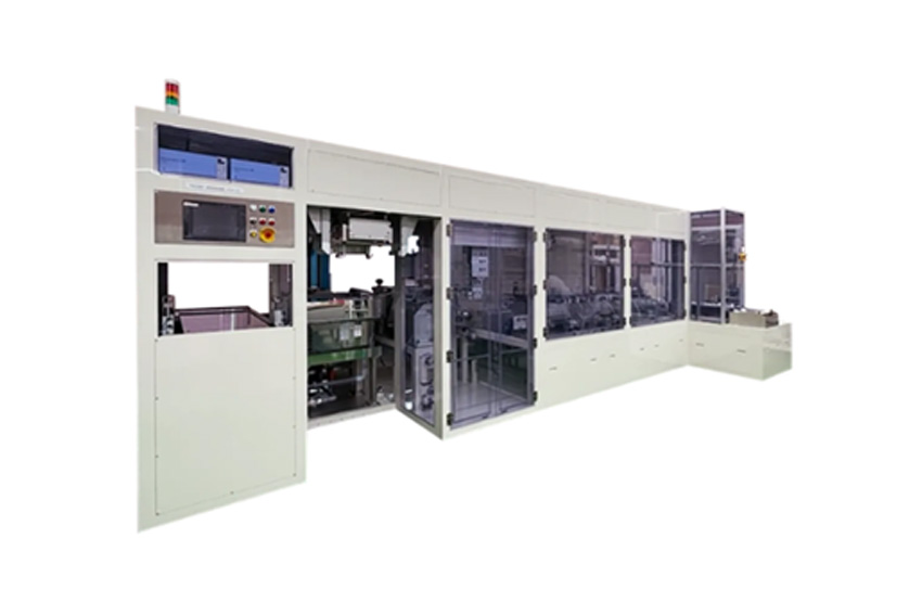
PWD2020 Automatic Wafer Demounter( demounting and cleaning)
We have automated our systems to increase productivity so that we can accommodate the mass production of semiconductors by our clients. Increasing speed and productivity as well as our quality is essential to our development. At the same time, diversifying our production bases and sales sites is necessary to cater to the globalization of semiconductor production. The US is our current target. As you have mentioned there are geopolitical reasons behind encompassing the semiconductor supply chain within the US. Stable supply and procurement are essential. Therefore, having a local base in the US and providing a stable supply is the next step that our company wants to take.
As enterprises attempt to diversify their production bases, industry leaders are increasingly viewing Japan as an alternative for cheap production and research. On top of IBM’s collaboration with Rapidus, Japan has attracted investments from major foundries. This includes TSMC’s new fabrication plant in Kyushu as well as investments from Micron Technology and Western Digital among others. According to industry experts, Japan’s advanced ecosystems in semiconductor materials and equipment are a strategic advantage for bringing production onshore. What are the comparative advantages of Japan as a production and research hub, and how do you expect the onshoring of cheap production to affect Japan’s semiconductor system?
There has been an active investment from mega semiconductor foundries such as TSMC from Taiwan, and Intel and Micron Technology from the US. These companies are attracted by the ecosystem that the Japanese semiconductor industry has. Traditionally, Japan has been well-known for its semiconductor production. Although this strength has shifted over the years, currently, Japan’s strength lies in the fields of material supply and equipment supply.
The Japanese government has taken a strong lead when it comes to Japan’s semiconductor industry. In June 2021, there was an announcement by Japan’s Ministry of Economy, Trade and Industry (METI) on the digital strategy of the semiconductor industry. This was the push that led to the flourishment of the industry. The government has been taking the lead from the economic security perspective. Since there is a huge demand internally within Japan especially due to Japan’s strong automotive market, there is a continuous need for semiconductors. Therefore, having domestic semiconductor production capabilities supports the other Japanese industries and is essential for economic security. For example, the Japanese government has been providing subsidies for foundries, and half of the construction costs for TSMC’s foundry were covered by these subsidies. This active involvement by the Japanese government is leading to the strengthening of Japan’s semiconductor ecosystem.
From TSMC’s perspective, there are currently geopolitical issues between China and Taiwan. Mitigating these types of geopolitical risks is essential for the stability of the global supply chain. TSMC chose Japan for that reason. The Samsung and SK group are also now looking to expand into Japan. TSMC’s facilities are located in Kyushu in southern Japan, while Rapidus’ facilities are located in Hokkaido in the north. However, the diversification of semiconductor bases has seen companies such as Samsung and SK Group investing more in the Tokyo and wider Kanto area. Domestically in Japan, the production sites have been dispersed to mitigate the high risks of natural disasters in Japan. Having multiple mega-foundries in Japan brings many advantages to the Japanese ecosystem. The first is a more complete supply chain and not having to be reliant on overseas markets for chips. This is essential for the stability of the Japanese economy. This also helps other Japanese companies to grow. At the same time, the dispersal of production sites in Japan is contributing to regional revitalization and creating new job opportunities and new industries in those regions, which of course is helping the Japanese economy to grow.
Having a flourishing Japanese semiconductor ecosystem also leads to technological advancement. This is pushing Japanese companies to invest in research and development and collaboration amongst the companies is creating innovations and providing new opportunities to go abroad with strengthened semiconductor products. Our company is actively engaged in collaboration with other companies as well as academia. For example, we have a collaboration with Top Universities from Japan and USA and we are now openly working on patenting our technology and formulating academic papers. This is helping us to showcase our technology and expand our presence.
One of your outstanding products is your wafer transfer devices. However, to adapt to the demand, some challenges remain. The transition to larger wafers represents challenges in terms of increased weight and potential handling issues. Ensuring precise and high-speed transportation for these larger wafers is crucial. It also demands extreme precision and reliability in wafer transportation to maintain the integrity of the delicate silicon wafer. Any deviation in handling could lead to defects and damage impacting the overall manufacturing process. The challenge lies in developing a transfer device that can seamlessly adapt to diverse types of variations. What specific features or technologies are incorporated to guarantee the precision and reliability of the wafer transfer, and how does the PWT2020 minimize the risks of errors, misalignment, or damage during transportation?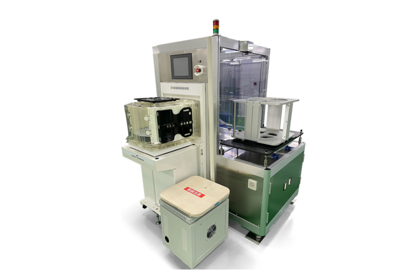
Wafer Transfer System PWT2020
Our company is derived from Phoenix Engineering which was established in 1980. We have over 44 years of experience in automation and robotics. One of the main strengths of our robot is that it can be maneuvered 360 degrees, which gives it an extensive operability range. We also have a demounting and peeling device embedded in the structure which is one of the niches of our device. On top of this, we have a device for temperature monitoring as well as the ability to exchange cassettes. The interface is intuitive and easy to operate. These advantages are included in our PWD2020 series which caters to various types of wafers including conventional silicon wafers as well as silicon carbide and gallium nitrate which is the next generation of high-power semiconductors.
Many features ensure the safety of the operation and mitigate the damage to the wafers. For example, we have emergency stop features, both physical and automatic. It can run at speeds of 200kmph which can be stopped suddenly without damaging the wafers that are being transported. These types of safety measures ensure safe operations. The cassette exchange features reduce abrasions and the risk of dust entering. Our PWT2020 also has the capability for in-carrier and out-of-carrier transportation as well as sensor and laser detection which reads the status of the wafer and determines what type of wafer it is. The sensor recognizes and monitors the environment. The PWT2020 provides the most adequate transportation for the different types of wafers that need to be transported.
The cylindrical coordinate clean robot PHT-R-4 is designed for precision handling in clean room environments and specifically for transporting delicate items such as 300mm wafers. The challenges include ensuring the robot's precise and rapid movement across multiple axes while maintaining a controlled environment. Additionally, the robot must also accommodate variations in workpieces, shapes, and materials demanding flexibility in handling metals. How does this product address the challenges of maintaining precision in the clean room environment, and are there features or technologies in place to minimize particle generation during the operation?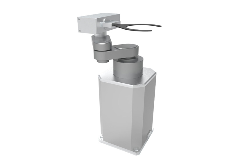
Wafer Transfer Robot PHT-R-4
The strength of our PHT-R-4 device is that it is customizable. We have been providing different features according to the needs of our customers. Our constant research and development make our products unique and ensure that we can provide innovative features. Of course, R&D takes time. Collaborating with our partners has helped us to provide new additional innovative features. Adding a fan at the bottom was one of the features that ensured the longer operability of the device. There is a growing need for semiconductors with the advent of AI. With that, new types of semiconductors are required. We have been working together with our partners and customers to develop a 450mm wafer handling device which is 18in. That will be our next focus in the growing AI market. Working together with our customers to understand their needs as well as the needs of the industry is important for continuously innovating our devices and equipment to cater to the rapidly changing semiconductor industry.
You have mentioned the importance that partnerships play. When we conducted interviews with other key players in the industry, they emphasized the importance of finding local partners to codevelop products and enhance their productivity and competitiveness in the international market. For example, we know that you collaborated with Gunma Industrial Technology Center to develop a transport robot that can handle large silicon wafers used for next-generation semiconductor equipment. You also mentioned that you collaborate with Top Universities from Japan and USA. Can you explain the role that partnerships play within your business model, and are you currently looking for new partners, especially in the overseas market?
Partnerships play a vital role in our business model. This is especially the case when it comes to procurement and production as we cooperate with multiple companies including parts manufacturers and electric appliance providers for example. There are many different companies involved in our product production. We want to expand our supply chain overseas so that we can conduct local production there. For example, I was recently in the US for one month to approach potential suppliers and customers. I showed our latest technology and explained the strengths and uniqueness of the products that we have. We also attend exhibitions to find customers and suppliers. On top of this, there are networking events that we attend.
Working with and through universities expands our scope for communication with other global semiconductor players. Joint research with universities is also key for elevating our technology and enhancing our global network. At the moment, our focus is on the US and Taiwan. However, soon, our vision is to expand to Korea and Europe. Last November, a major European wafer maker visited our factory and studied our latest automated wafer transportation and cleaning devices. Although we have not yet reached an agreement on a partnership, they are constantly interested in knowing our latest news. The American and European way of establishing partnerships is different from how it is done in Japan. For the US and Europe, it is more about the long-term sharing of information and understanding of technology. We are trying to acquire a presence in both the US and Europe.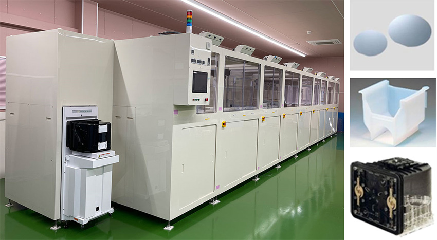
SCC-250 Wafer Cleaner
Your company is this year celebrating its 44th anniversary. Imagine that we come back six years from now for your 50th anniversary. What goals would you like to achieve over the next six years, and what message would you like to send to plausible partners who will read this report?
My vision for the upcoming six years is to first expand in the domestic market. We need to have a robust network within Japan, not only in the Kanto area but also in Kyushu and the Tohoku area. This will allow us to cater to the regional needs of the industry. At the same time, we want to ensure a stable acquisition of talented individuals as increasing the capabilities of our human resources is very important. We want to continue collaborating with universities, research centers, and governmental entities to secure highly talented individuals for creating innovations.
Growing overseas is key to the growth of the company. As I mentioned, our current focus is on the US. We acquired an American precision machined parts manufacturer (ADVANCED SPECIAL TOOLS INC.-URL: https://astindex.com/ ), which is a US joint venture between a Japanese precision ceramic parts company and Mitsubishi Aluminum. That is the next market for us. Having a local production base, supply chain, and sales channel is important for us in that regard. Establishing our entity in the US is key to our evolution. Aside from the US, we are also focusing on the Asian region. We currently have a base in China, and we are looking to expand our presence to Taiwan and Korea and set up bases there. We are now in discussions with a Taiwan regional bank to establish a local factory there and contribute to the local semiconductor industry. Our long-term vision is to be a listed company and be recognized as an attractive asset for investment funds, asset management companies, and mega banks. We want to be known as a reliable company that contributes to society. They are my goal for the future.
For more details, explore their website at https://pht.co.jp/en/
The Worldfolio provides business, industrial and financial news about global economies, with a focus on understanding them from within.
PUBLICATIONS
DATABASE
ABOUT
SOCIAL MEDIA